LH540203U-20 Ver la hoja de datos (PDF) - Sharp Electronics
NГәmero de pieza
componentes DescripciГіn
Fabricante
LH540203U-20 Datasheet PDF : 17 Pages
| |||
LH540203
FUNCTIONAL DESCRIPTION (contвҖҷd)
Data words are read out from the LH540203вҖҷs output
port in precisely the same order that they were written in
at its input port; that is, according to a First-In, First Out
(FIFO) queue discipline. Since the addressing sequence
for a FIFO deviceвҖҷs memory is internally predefined, no
external addressing information is required for the opera-
tion of the LH540203 device.
Drop-in-replacement compatibility is maintained with
both larger sizes and smaller sizes of industry-standard
nine-bit asynchronous FIFOs. The only change is in the
number of internally-stored data words implied by the
states of the Full Flag and the Half-Full Flag.
The Retransmit (RT) control signal causes the internal
FIFO-memory-array read-address pointer to be set back
to zero, to point to the LH540203вҖҷs first physical memory
location, without affecting the internal FIFO-memory-
array write-address pointer. Thus, the Retransmit control
signal provides a mechanism whereby a block of data,
delimited by the zero physical address and the current
write-address-pointer value, may be read out repeatedly
an arbitrary number of times. The only restrictions are that
neither the read-address pointer nor the write-address
pointer may вҖҳwrap aroundвҖҷ during this entire process, i.e.,
advance past physical location zero after traversing the
entire memory. The retransmit facility is not available
when an LH540203 is operating in a depth-expanded
configuration.
CMOS 2048 Г— 9 Asynchronous FIFO
The Reset (RS) control signal returns the LH540203
to an initial state, empty and ready to be filled. An
LH540203 should be reset during every system power-up
sequence. A reset operation causes the internal FIFO-
memory-array write-address pointer, as well as the read-
address pointer, to be set back to zero, to point to the
LH540203вҖҷs first physical memory location. Any informa-
tion which previously had been stored within the
LH540203 is not recoverable after a reset operation.
Acascading (depth-expansion) scheme may be imple-
mented by using the Expansion In (XI) input signal and
the Expansion Out (XO/HF) output signal. This allows a
deeper вҖҳeffective FIFOвҖҷ to be implemented by using two
or more LH540203 devices, without incurring additional
latency (вҖҳfallthroughвҖҷ or вҖҳbubblethroughвҖҷ) delays, and with-
out the necessity of storing and retrieving any given data
word more than once. In this cascaded operating mode,
one LH540203 device must be designated as the вҖҳfirst-
loadвҖҷ or вҖҳmasterвҖҷ device, by grounding its First-Load
(FL/RT) control input; the remaining LH540203 devices
are designated as вҖҳslaves,вҖҷ by tying their FL/RT inputs
HIGH. Because of the need to share control signals on
pins, the Half-Full Flag and the retransmission capability
are not available for either вҖҳmasterвҖҷ or вҖҳslaveвҖҷ LH540203
devices operating in cascaded mode.
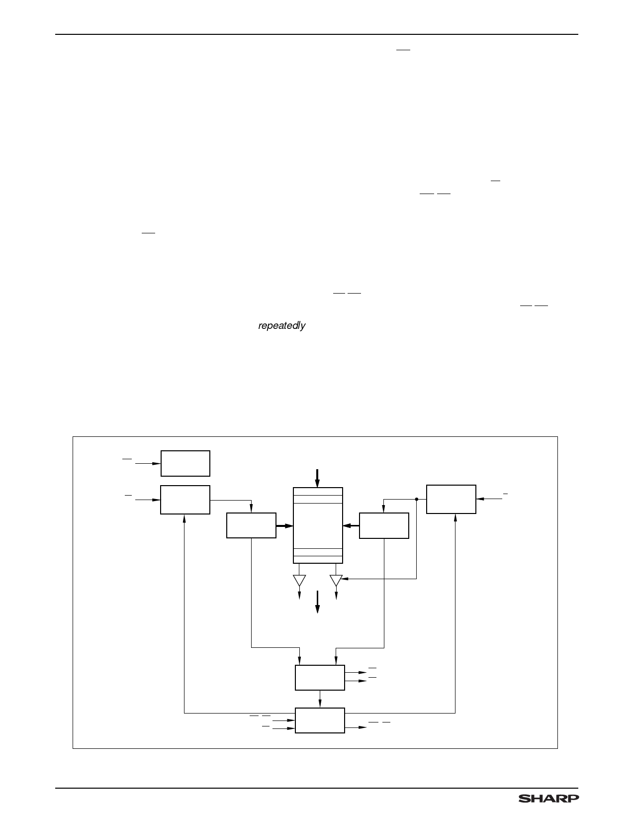
RS
RESET
LOGIC
DATA INPUTS
D0 - D8
INPUT
OUTPUT
W
PORT
PORT
R
CONTROL
DUAL-PORT
CONTROL
WRITE
POINTER
RAM
ARRAY
READ
POINTER
2048 x 9
...
DATA OUTPUTS
Q0 - Q8
FLAG
EF
LOGIC
FF
FL/RT
XI
EXPANSION
LOGIC
XO/HF
Figure 3. LH540203 Block Diagram
540203-1
2
Share Link: 