LC75836W Ver la hoja de datos (PDF) - SANYO -> Panasonic
Número de pieza
componentes Descripción
Fabricante
LC75836W Datasheet PDF : 18 Pages
| |||
LC75836W
Electrical Characteristics for the Allowable Operating Ranges
Parameter
Symbol
Pin
Conditions
Ratings
Unit
min
typ
max
Hysteresis
Input high-level current
VH
CE, CL, DI, INH
IIH1
CE, CL, DI, INH VI = 6.0V
IIH2
OSC
VI = VDD external clock operating mode
0.03VDD
V
5.0
μA
5.0
Input low-level current
IIL1
CE, CL, DI, INH VI = 0V
-5.0
μA
IIL2
OSC
VI = 0V external clock operating mode
-5.0
Output high-level voltage VOH1 S1 to S35
IO = -20μA
VDD-0.9
VOH2
COM1
to COM4
IO = -100μA
VDD-0.9
V
Output low-level voltage
VOH3
VOL1
P1 to P4
S1 to S35
IO = -1mA
IO = 20μA
VDD-0.9
0.9
VOL2
COM1
to COM4
IO = 100μA
0.9 V
VOL3 P1 to P4
IO =1mA
0.9
Output middle-level
voltage *1
VMID1 S1 to S35
1/3 bias IO = ±20μA
2/3VDD
-0.9
2/3VDD
+0.9
VMID2 S1 to S35
VMID3
COM1
to COM4
1/3 bias IO = ±20μA
1/3 bias IO = ±100μA
1/3VDD
-0.9
2/3VDD
-0.9
1/3VDD
+0.9
V
2/3VDD
+0.9
VMID4
COM1
to COM4
1/3 bias IO = ±100μA
1/3VDD
-0.9
1/3VDD
+0.9
Oscillator frequency
fosc OSC
RC oscillator operating mode
Rosc = 39 kΩ, Cosc = 1000pF
30.4
38
45.6 kHz
Current drain
IDD1 VDD
Power-saving mode
5
IDD2 VDD
VDD = 6.0V output open
RC oscillator operating mode
350
700
fosc = 38kHz
IDD3 VDD
VDD = 6.0V output open
μA
External clock operating mode
fCK = 38kHz
450
900
VIH2 = 0.5VDD
VIL2 = 0.1VDD
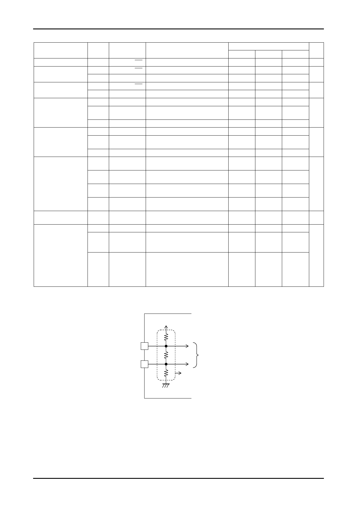
Note: *1 Excluding the bias voltage generation divider resistors built in the VDD1 and VDD2. (See Figure 1.)
VDD1
VDD2
VDD
To the common and segment drivers
Except these resistors.
VSS
Figure 1
No.A0428-3/18
Share Link: 