LC72151V Ver la hoja de datos (PDF) - SANYO -> Panasonic
Número de pieza
componentes Descripción
Fabricante
LC72151V Datasheet PDF : 29 Pages
| |||
LC72151V
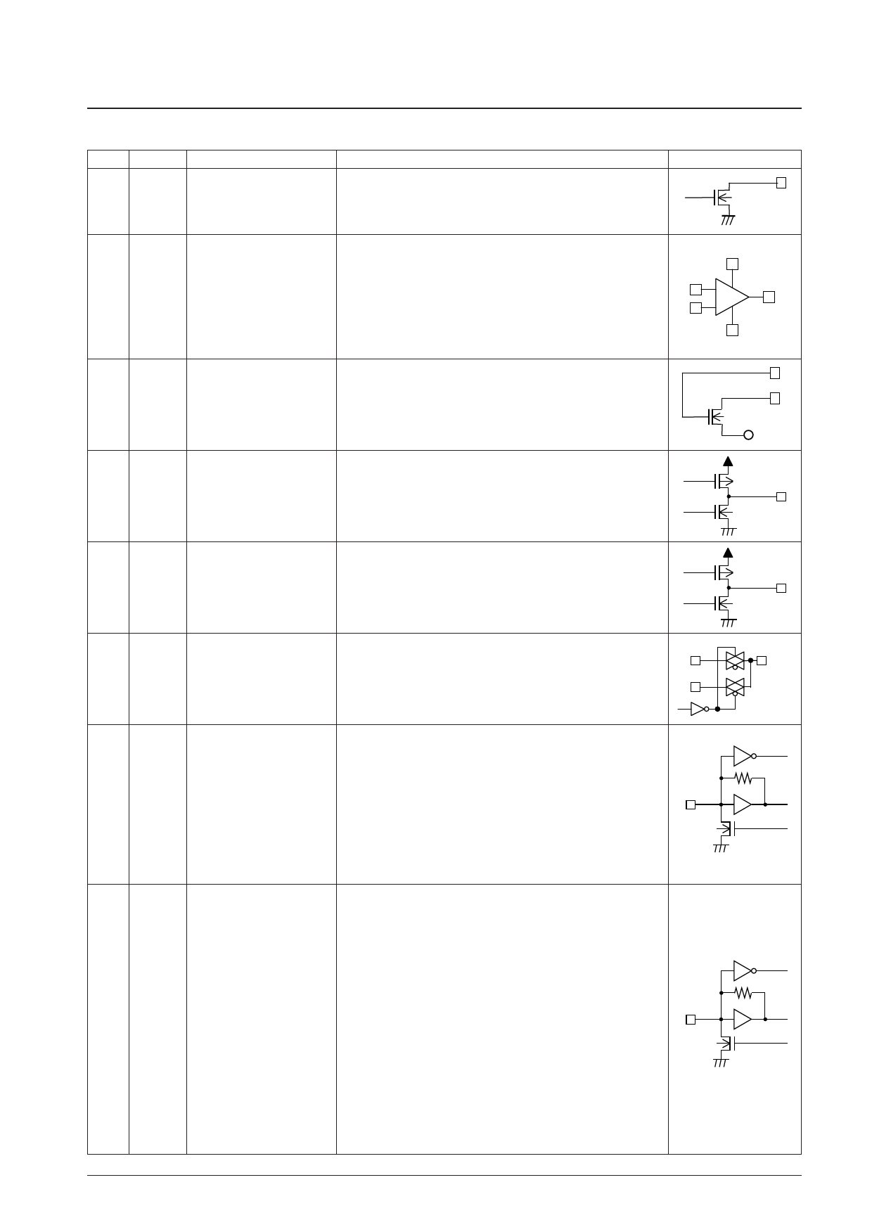
Continued from preceding page.
Pin No. Symbol
5
O-3
Usage
Output port
Function
• Dedicated output pin
• Latches OUT3 in the control data and outputs data from O-3 pin.
• This pin goes open state at a power-on reset.
Pin circuit
19
AIN1
• Op-amp for PLL active low-pass filter
AVDD
12
AREF
• AVSS is the analog system ground pin shared with low-pass filter Nch AIN1
13
14
15
AVDD
AVSS
AOUT1
MOS transistor.
Op-amp for low-pass filter amp
• Voltage applied to AREF pin must be 1/2 that to VDD pin.
Note: Power must be applied to AVDD before applied to VDD, and AVDD
must be higher than or equal to VDD.
–
+
AREF
AOUT1
AVSS
24
AIN2
25
AOUT2
Transistor for low-pass
filter amp
• PLL active low-pass filter Nch MOS transistor
• Source of the transistor is connected to AVSS pin.
Note: Connect AVSS pin to ground in use.
21
PDM1
23
PDM2
20
PDS
Charge pump output
• PLL charge pump output
When the frequency created by dividing the local oscillator signal
frequency by N is higher than the reference frequency, a high level is
output from the PD pin. When lower, a low level is output. The PD pin
goes to the high-impedance state when the frequencies match.
AVSS
• PLL high-speed locking charge pump output
22
PDF
PLL high-speed locking charge When the high-speed locking mode is selected, signal pulses is
pump output
output according to the frequency variation. This pin enters high-
impedance state when the local oscillation frequency enters the set
frequency range.
18
TGI1
TGI1
• PLL high-speed locking active low-pass filter transmission gate
17
TGI2
PLL high-speed locking TG
input/output dual function pins
TGI2
16
TGO
Note: Connect AVSS pin to ground in use.
TGO
10 HCTR/I-3
11 LCTR/I-4
General-purpose counter
General-purpose counter
• HCTR is selected by setting CTS1 in the control data to 1.
Input frequency: 0.4 to 25 MHz
The signal is input to a divide-by-2 circuit and the result is input to a
general-purpose counter. This counter can also be used as an
integrating counter.
The counter value is output as the result of the count, MSB first, from
the DO pin.
There are four measurement periods: 4, 8, 32, and 64 ms.
• When H/I-3 in the control data is set, this pin functions as an input
port, and the value is output from the output pin DO.
• LCTR is selected by setting CTS1 in the control data to 1.
• When the LCTR is selected as described above and CTS0 is set to 1:
This pin enters the frequency measurement mode.
Input frequency: 10 to 500 kHz
The signal is directly transmitted to the general-purpose counter.
• When CTS0 is set to 0
This pin enters period measurement mode.
Input frequency: 1 Hz to 20 kHz
Period can be measured either in single period or in double period. If
double period measurement is selected, the frequency is 2 Hz to
40 kHz.
The counter value is output as the result of the count, MSB first, from
the DO pin.
• When L/I-4 in the control data is set:
This pin functions as an input port, the value is output from the output
pin DO.
Continued on next page.
No. 6976-8/29
Share Link: 