LB1928(1999) Ver la hoja de datos (PDF) - SANYO -> Panasonic
Número de pieza
componentes Descripción
Fabricante
LB1928
(Rev.:1999)
(Rev.:1999)
SANYO -> Panasonic

LB1928 Datasheet PDF : 11 Pages
| |||
Continued from preceding page
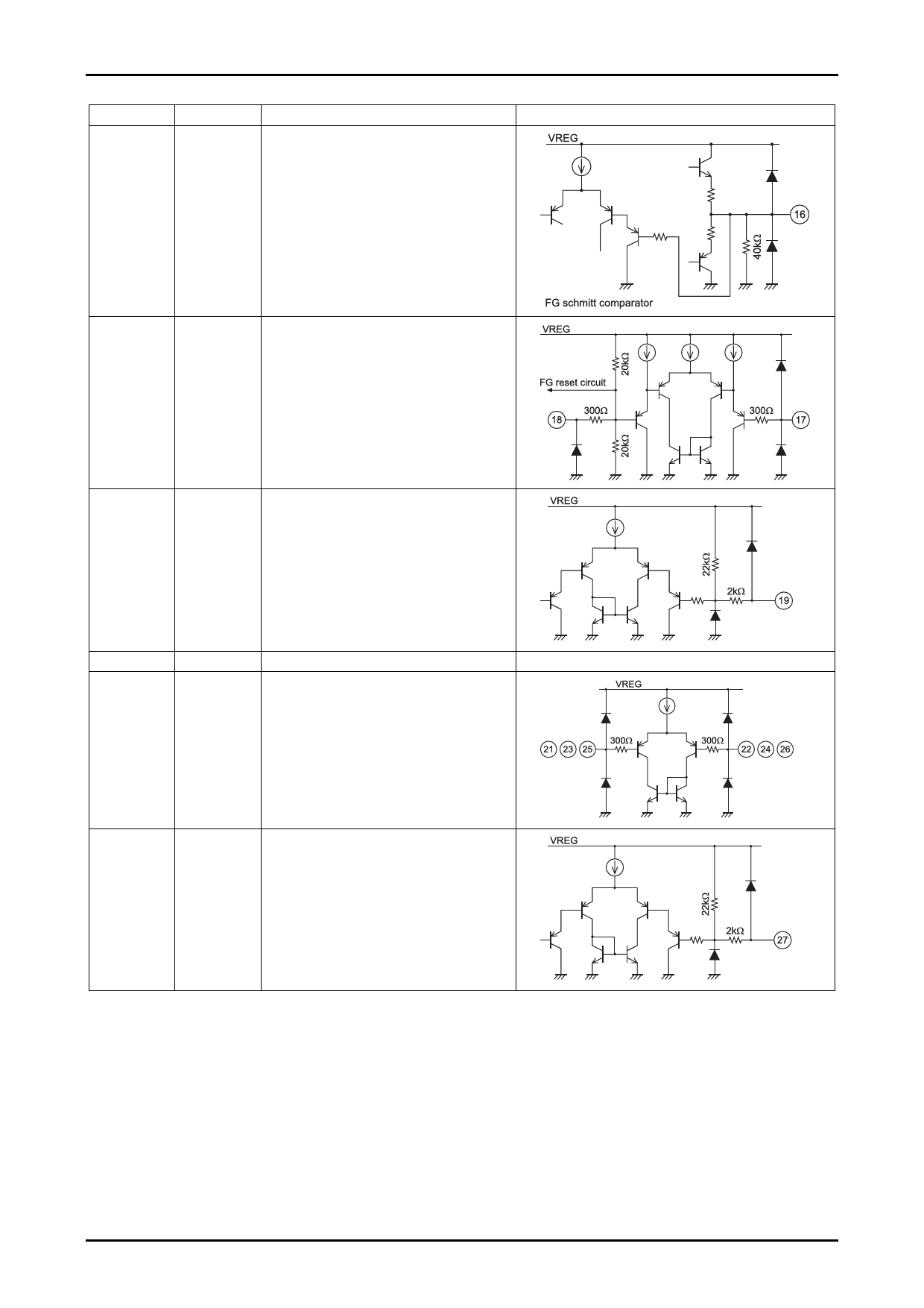
Pin number Pin name
16
FG
OUT
VREG
LB1928
Equivalent circuit
16
Pin function
FG amplifier output pin.
17
FGIN–
18
FGIN+
19
S/S
20
GND1
22
IN1+
21
IN1–
24
IN2+
23
IN2–
26
IN3+
25
IN3–
27
F/R
FG schmitt comparator
VREG
FG reset circuit
300Ω
18
VREG
VREG
300Ω
21 23 25
VREG
A12993
300Ω
17
FG amplifier input pin.
By connecting a capacitor (approx. 0.1 µF)
between FGIN+ and ground, the logic circuitry
is reset.
A12994
2kΩ
19
A12995
Start/stop control pin.
Start (Low): 0V to 1.5V
Stop (High): 3.5V to VREG
High when open.
Hysteresis width: approx. 0.5V.
300Ω
22 24 26
Ground pin (except for output block).
Hall input pins.
High when IN+ > IN–, Low when IN+ < IN–.
Hall signal should have an amplitude of at least
100 mVp–p (differential operation). When Hall
signal noise is a problem, connect a capacitor
between IN+ and IN–.
A12996
2kΩ
27
A12997
Forward/reverse control pin.
Forward (Low): 0V to 1.5V
Reverse (High): 3.5V to VREG
High when open.
Hysteresis width: approx. 0.5V.
No. 6198-8/11
Share Link: