LB1695D Ver la hoja de datos (PDF) - SANYO -> Panasonic
Número de pieza
componentes Descripción
Fabricante
LB1695D Datasheet PDF : 10 Pages
| |||
LB1695D
Pin Description
Pin name
VCC
R
C
NC
OUT1
OUT2
OUT3
RF
VM
GND
F/R
IN1+, IN1–
IN2+, IN2–
IN3+, IN3–
FG1
FG2
Pin number
1
2
3
4, 9
5
6
7
8
10
11
12
17, 18
15, 16
13, 14
20
19
Function
Power supply pin for blocks except output
C pin charge/discharge current set pin
Setting pin for current limiter output off time and output current ignore time
May be used for wiring
Output pin 1
Output pin 2
Output pin 3
Output current detection pin. Insert a resistor (Rf) between this pin and ground.
The output current will be limited to the value determined by VRF/Rf (output current limiter).
Power supply pin for output
Ground for blocks except output
Lowest electrical potential of output transistors is voltage at RF pin.
Forward/reverse control pin
Hall input pin Logic High refers to IN+ > IN–
Hall input pin Logic High refers to IN+ > IN–
Hall input pin Logic High refers to IN+ > IN–
Speed pulse output pin 1 with built-in pull-up resistor
Speed pulse output pin 2 with built-in pull-up resistor
Pin Assignment
FG1 FG2 IN1– IN1+ IN2– IN2+ IN3– IN3+ F/R GND
20 19 18 17 16 15 14 13 12 11
LB1695D
1 2 3 4 5 6 7 8 9 10
VCC R C NC OUT1OUT2 OUT3 RF NC VM
Top view
24
20
16
12
8
4
3
0 –20
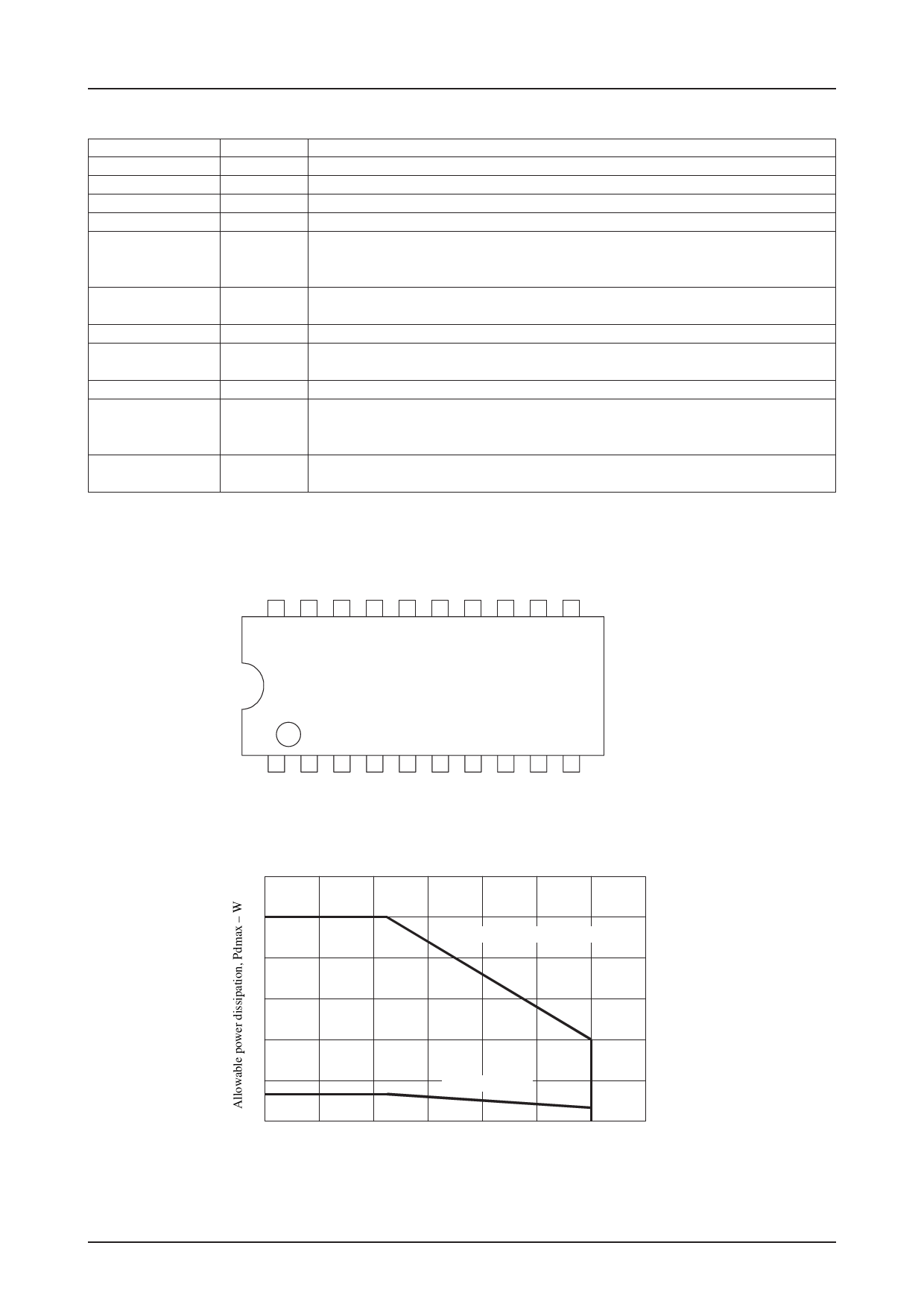
0
Pdmax – Ta
With an arbitrary large heat sink
8.0W
Without heat sink
20
40
60
80
Ambient temperature, Ta – °C
1.2W
100
120
No. 6205-4/10
Share Link: 