LA7265W(1998) Ver la hoja de datos (PDF) - SANYO -> Panasonic
Número de pieza
componentes Descripción
Fabricante
LA7265W Datasheet PDF : 24 Pages
| |||
LA7265W
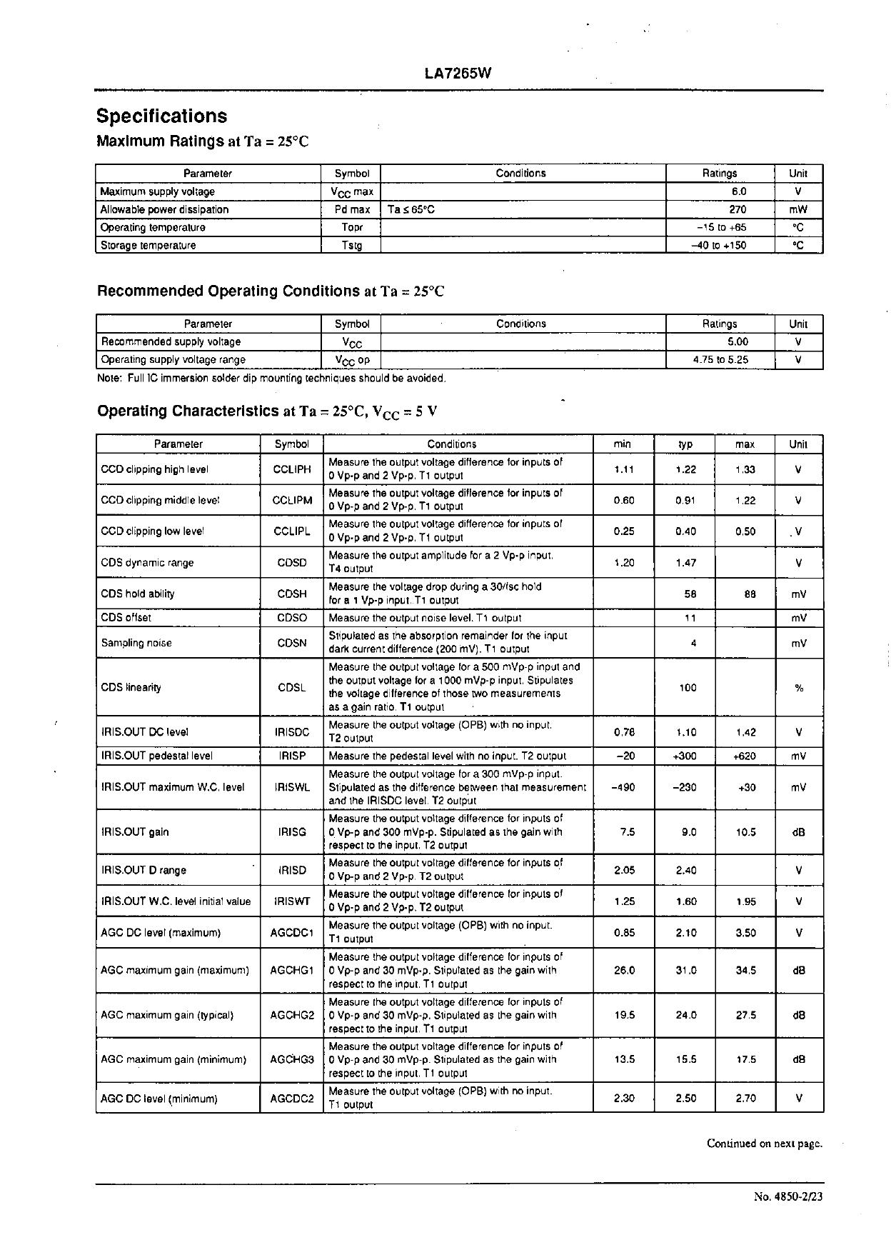
Specifications
Maximum Ratings at Ta = 25°C
Parameter
Maximum supply voltage
Allowable power dissipation
Operating temperature
Storage temperature
Symbol
VCC max
Pd max
Topr
Tstg
Ta ≤ 65°C
Recommended Operating Conditions at Ta = 25°C
Parameter
Symbol
Recommended supply voltage
VCC
Operating supply voltage range
VCC op
Note: Full IC immersion solder dip mounting techniques should be avoided.
Operating Characteristics at Ta = 25°C, VCC = 5 V
Conditions
Conditions
Parameter
Symbol
Conditions
CCD clipping high level
CCD clipping middle level
CCD clipping low level
CDS dynamic range
CDS hold ability
CDS offset
Sampling noise
CDS linearity
IRIS.OUT DC level
IRIS.OUT pedestal level
IRIS.OUT maximum W.C. level
IRIS.OUT gain
IRIS.OUT D range
IRIS.OUT W.C. level initial value
AGC DC level (maximum)
AGC maximum gain (maximum)
AGC maximum gain (typical)
AGC maximum gain (minimum)
AGC DC level (minimum)
CCLIPH
CCLIPM
CCLIPL
CDSD
CDSH
CDSO
CDSN
CDSL
IRISDC
IRISP
IRISWL
IRISG
IRISD
IRISWT
AGCDC1
AGCHG1
AGCHG2
AGCHG3
AGCDC2
Measure the output voltage difference for inputs of
0 Vp-p and 2 Vp-p. T1 output
Measure the output voltage difference for inputs of
0 Vp-p and 2 Vp-p. T1 output
Measure the output voltage difference for inputs of
0 Vp-p and 2 Vp-p. T1 output
Measure the output amplitude for a 2 Vp-p input.
T4 output
Measure the voltage drop during a 30/fsc hold
for a 1 Vp-p input. T1 output
Measure the output noise level. T1 output
Stipulated as the absorption remainder for the input
dark current difference (200 mV). T1 output
Measure the output voltage for a 500 mVp-p input and
the output voltage for a 1000 mVp-p input. Stipulates
the voltage difference of those two measurements
as a gain ratio. T1 output
Measure the output voltage (OPB) with no input.
T2 output
Measure the pedestal level with no input. T2 output
Measure the output voltage for a 300 mVp-p input.
Stipulated as the difference between that measurement
and the IRISDC level. T2 output
Measure the output voltage difference for inputs of
0 Vp-p and 300 mVp-p. Stipulated as the gain with
respect to the input. T2 output
Measure the output voltage difference for inputs of
0 Vp-p and 2 Vp-p. T2 output
Measure the output voltage difference for inputs of
0 Vp-p and 2 Vp-p. T2 output
Measure the output voltage (OPB) with no input.
T1 output
Measure the output voltage difference for inputs of
0 Vp-p and 30 mVp-p. Stipulated as the gain with
respect to the input. T1 output
Measure the output voltage difference for inputs of
0 Vp-p and 30 mVp-p. Stipulated as the gain with
respect to the input. T1 output
Measure the output voltage difference for inputs of
0 Vp-p and 30 mVp-p. Stipulated as the gain with
respect to the input. T1 output
Measure the output voltage (OPB) with no input.
T1 output
min
1.11
0.60
0.25
1.20
0.78
–20
–490
7.5
2.05
1.25
0.85
26.0
19.5
13.5
2.30
Ratings
Unit
6.0
V
270
mW
–15 to +65
°C
–40 to +150
°C
Ratings
Unit
5.00
V
4.75 to 5.25
V
Ratings
Unit
typ
max
1.22
1.33
V
0.91
1.22
V
0.40
0.50
V
1.47
V
58
88
mV
11
mV
4
mV
100
%
1.10
1.42
V
+300
+620
mV
–230
+30
mV
9.0
10.5
dB
2.40
V
1.60
1.95
V
2.10
3.50
V
31.0
34.5
dB
24.0
27.5
dB
15.5
17.5
dB
2.50
2.70
V
Continued on next page.
No. 4850-2/24
Share Link: 