LA4809M Ver la hoja de datos (PDF) - SANYO -> Panasonic
Número de pieza
componentes Descripción
Fabricante
LA4809M Datasheet PDF : 15 Pages
| |||
LA4809M
7. Selection of the maximum output power value (handling of Pin 10)
This IC enables selection of two types of maximum output power value according to the handling method of Pin 10.
The regulator circuit for output power control is built in, in which, by changing the voltage of Pin 2, the regulator
voltage : Vreg is changed to enable selection of the maximum output power value.
Mode-A (PO max = 55mW) : Pin 10 set to the OPEN state
Pin 2 voltage : V2 = 2.1V,
Internal regulator voltage : Vreg = 4.2V,
Amplifier operating reference voltage : Vref = 2.1V
Mode-B (PO max = 160mW) : Pin 10 connected to the GND line
Pin 2 voltage : V2 = 3.1V,
Internal regulator voltage : Vreg = 6.2V,
Amplifier operation reference voltage : Vref = 3.1V
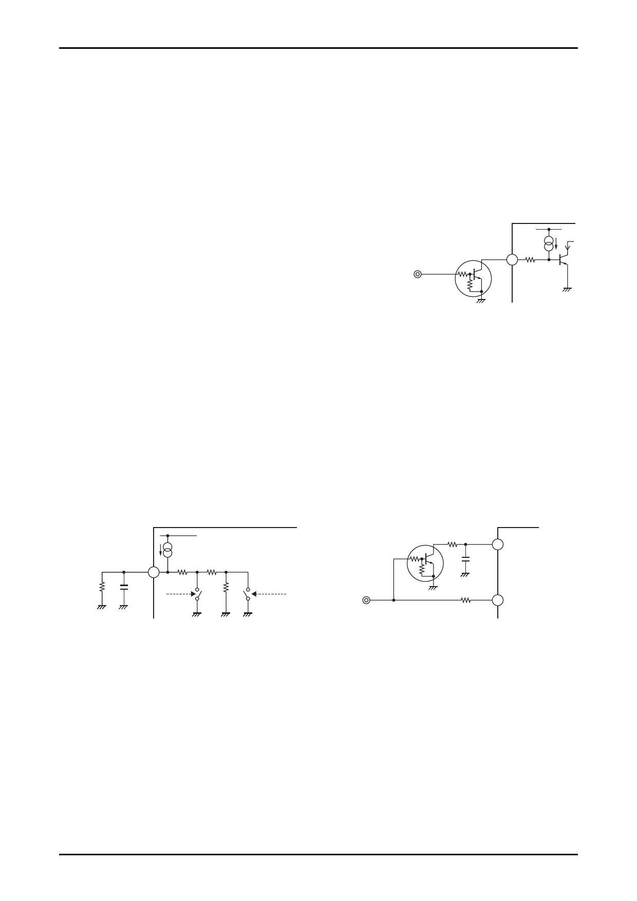
When the maximum output power value is to be changed under CPU
control, use the NPN transistor as shown in Fig.4, so that the Pin 10
voltage approaches the GND potential (0.1V or below) sufficiently.
VCC
PLS 22μA
10
10kΩ
from CPU
Fig.4
8. Change of the maximum output power value (by handling Pin 2)
Pin 2 voltage : V2 is determined from the constant-current source and internal resistance as shown in Fig.5.
Operating ⇒ Mode-A : 54kΩ used
Mode-B : 80kΩ (54kΩ + 26kΩ) used
Not operating (at a time of falling) ⇒ 157kΩ (54kΩ + 26kΩ + 77kΩ) used
The internal regulator voltage and amplifier operating reference voltage are generated from this Pin 2 voltage.
Regulator voltage : Vreg = V2 × 2
Amplifier operating reference voltage : Vref = V2 × 1
Accordingly, to change the maximum output power value, connect the resistance : Rrf between Pin 2 and GND as
shown in Fig.5. This will cause change in the Pin 2 voltage. Note that, in view of circuit operation, the Pin 2 voltage
must be set to 1.6V or above.
If the discharge constant is not to be changed, Use the NPN transistor to control the Rrf connection as shown in Fig.6.
VCC
39μA
RF 54kΩ 26kΩ
2
Rrf Crf
77kΩ
PLS-cnt
STBY-cnt
from CPU
Rrf
2 RF
Crf
3 STBY
Fig.5
Fig.6
9. Standby pin (Pin 3)
By controlling the standby pin, the mode can be changed over between standby and operation. Though this control is
possible directly by the CPU output port, the control may be exposed to adverse affect of digital noise from CPU. It is
recommended therefore to insert series resistance (1kΩ or more).
Standby mode ⇒ V3 = 0V to 0.6V
Operation mode ⇒ V3 = 2V to 9V (for VCC = 9V or above), V3 = 2V to VCC (for VCC = less than 9V)
Continued on next page.
No.A1569-7/15
Share Link: 