L6563 Ver la hoja de datos (PDF) - STMicroelectronics
Número de pieza
componentes Descripción
Fabricante
L6563 Datasheet PDF : 37 Pages
| |||
Description
1.1
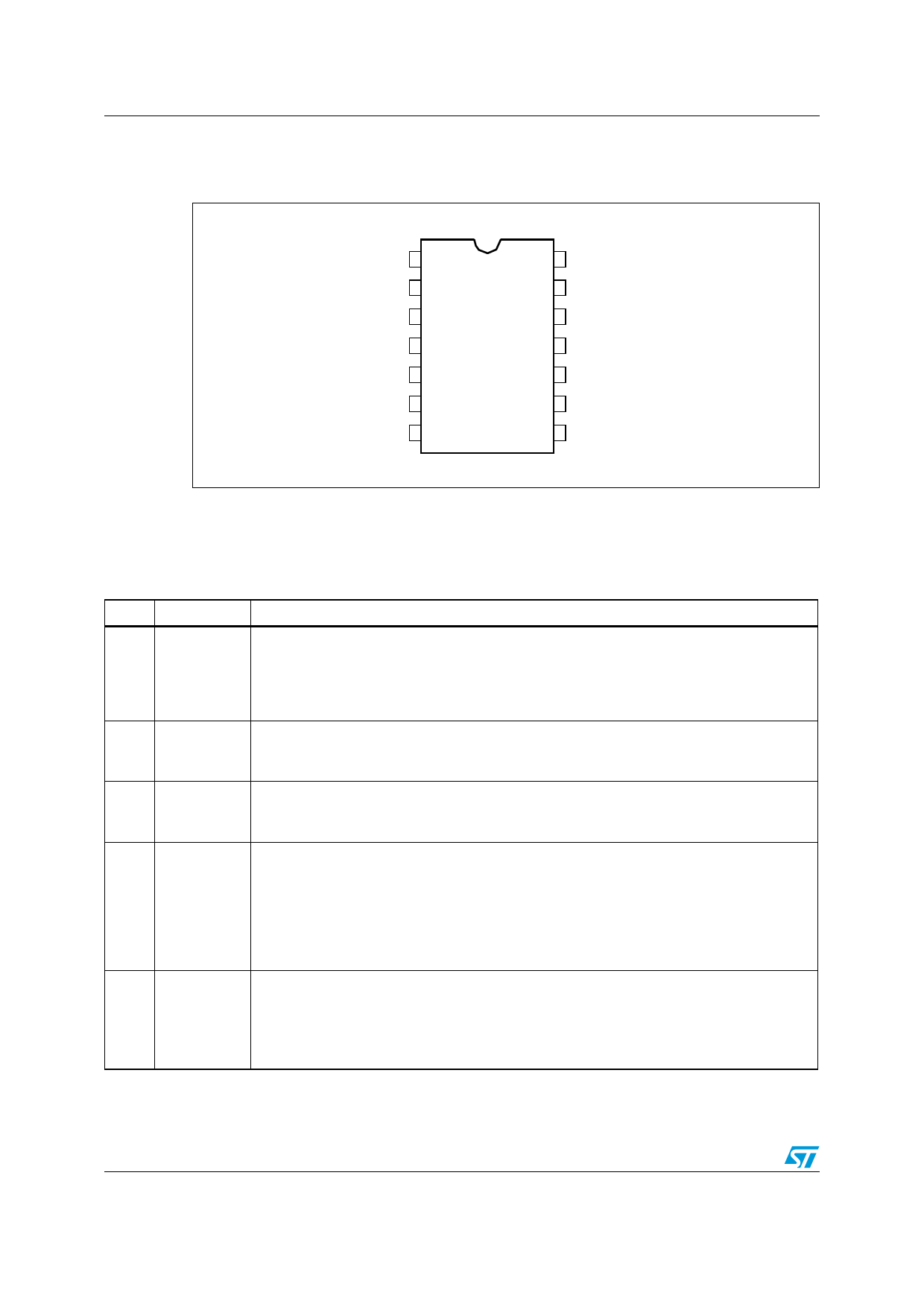
Pin connection
Figure 2. Pin connection (top view)
INV 1
COMP 2
MULT 3
CS 4
VFF 5
TBO 6
PFC_OK 7
L6563 - L6563A
14 Vcc
13 GD
12 GND
11 ZCD
10 RUN
9 PWM_STOP
8 PWM_LATCH
1.2
Pin description
Table 1. Pin description
Pin N° Name
Description
Inverting input of the error amplifier. The information on the output voltage of the PFC pre-
regulator is fed into the pin through a resistor divider.
1
INV
The pin normally features high impedance but, if the tracking boost function is used, an
internal current generator programmed by TBO (pin 6) is activated. It sinks current from the
pin to change the output voltage so that it tracks the mains voltage.
Output of the error amplifier. A compensation network is placed between this pin and INV
2
COMP (pin 1) to achieve stability of the voltage control loop and ensure high power factor and low
THD.
Main input to the multiplier. This pin is connected to the rectified mains voltage via a
3
MULT resistor divider and provides the sinusoidal reference to the current loop. The voltage on
this pin is used also to derive the information on the RMS mains voltage.
Input to the PWM comparator. The current flowing in the MOSFET is sensed through a
resistor, the resulting voltage is applied to this pin and compared with an internal reference
to determine MOSFET’s turn-off.
4
CS
A second comparison level at 1.7V detects abnormal currents (e.g. due to boost inductor
saturation) and, on this occurrence, shuts down the IC, reduces its consumption almost to
the start-up level and asserts PWM_LATCH (pin 8) high. This function is not present in the
L6563A.
Second input to the multiplier for 1/V2 function. A capacitor and a parallel resistor must be
connected from the pin to GND. They complete the internal peak-holding circuit that
5
VFF
derives the information on the RMS mains voltage. The voltage at this pin, a DC level equal
to the peak voltage at pin MULT (pin 3), compensates the control loop gain dependence on
the mains voltage. Never connect the pin directly to GND.
4/37
Share Link: 