L6563 Ver la hoja de datos (PDF) - STMicroelectronics
Número de pieza
componentes Descripción
Fabricante
L6563 Datasheet PDF : 37 Pages
| |||
L6563 - L6563A
1
Description
Description
The device is a current-mode PFC controller operating in Transition Mode (TM). Based on
the core of a standard TM PFC controller, it offers improved performance and additional
functions.
The highly linear multiplier, along with a special correction circuit that reduces crossover
distortion of the mains current, allows wide-range-mains operation with an extremely low
THD even over a large load range.
The output voltage is controlled by means of a voltage-mode error amplifier and a precise
(1.5% @TJ = 25°C) internal voltage reference. The stability of the loop and the transient
response to sudden mains voltage changes are improved by the voltage feedforward
function (1/V2 correction).
Additionally, the IC provides the option for tracking boost operation (where the output
voltage is changed tracking the mains voltage). The device features extremely low
consumption (≤90 µA before start-up and ≤5 mA running).
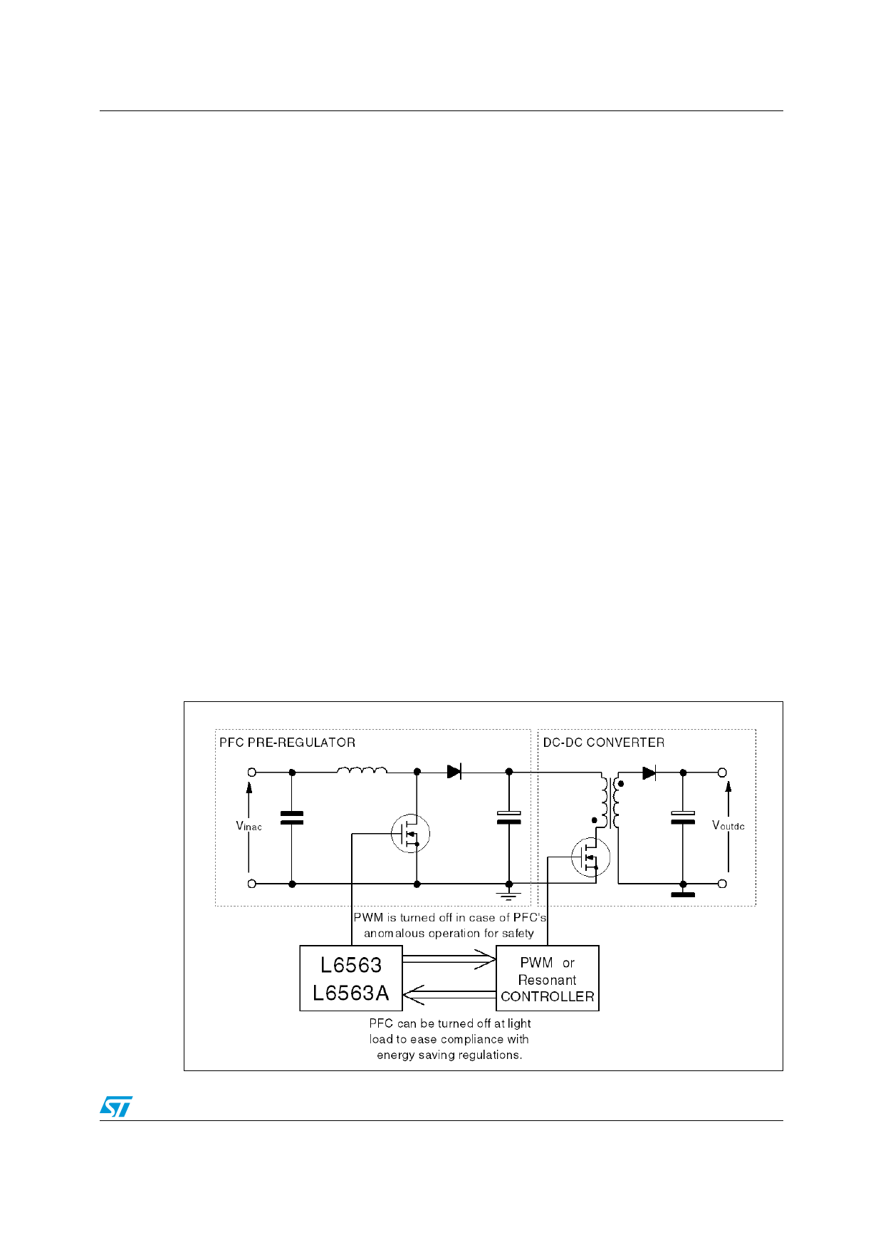
An interface with the PWM controller of the DC-DC converter supplied by the PFC pre-
regulator is provided: the purpose is to stop the operation of the converter in case of
anomalous conditions for the PFC stage (feedback loop failure, boost inductor's core
saturation) and to disable the PFC stage in case of light load for the DC-DC converter, so as
to make it easier to comply with energy saving norms (Blue Angel, EnergyStar, Energy2000,
etc.). The device includes disable functions suitable for remote ON/OFF control both in
systems where the PFC pre-regulator works as a master and in those where it works as a
slave.
In addition to an effective two-step OVP that handles normal operation overvoltages, the IC
provides also a protection against feedback loop failures or erroneous output voltage
setting.
Figure 1. Typical system block diagram
3/37
Share Link: 