L6562D Ver la hoja de datos (PDF) - STMicroelectronics
Número de pieza
componentes Descripción
Fabricante
L6562D Datasheet PDF : 16 Pages
| |||
L6562
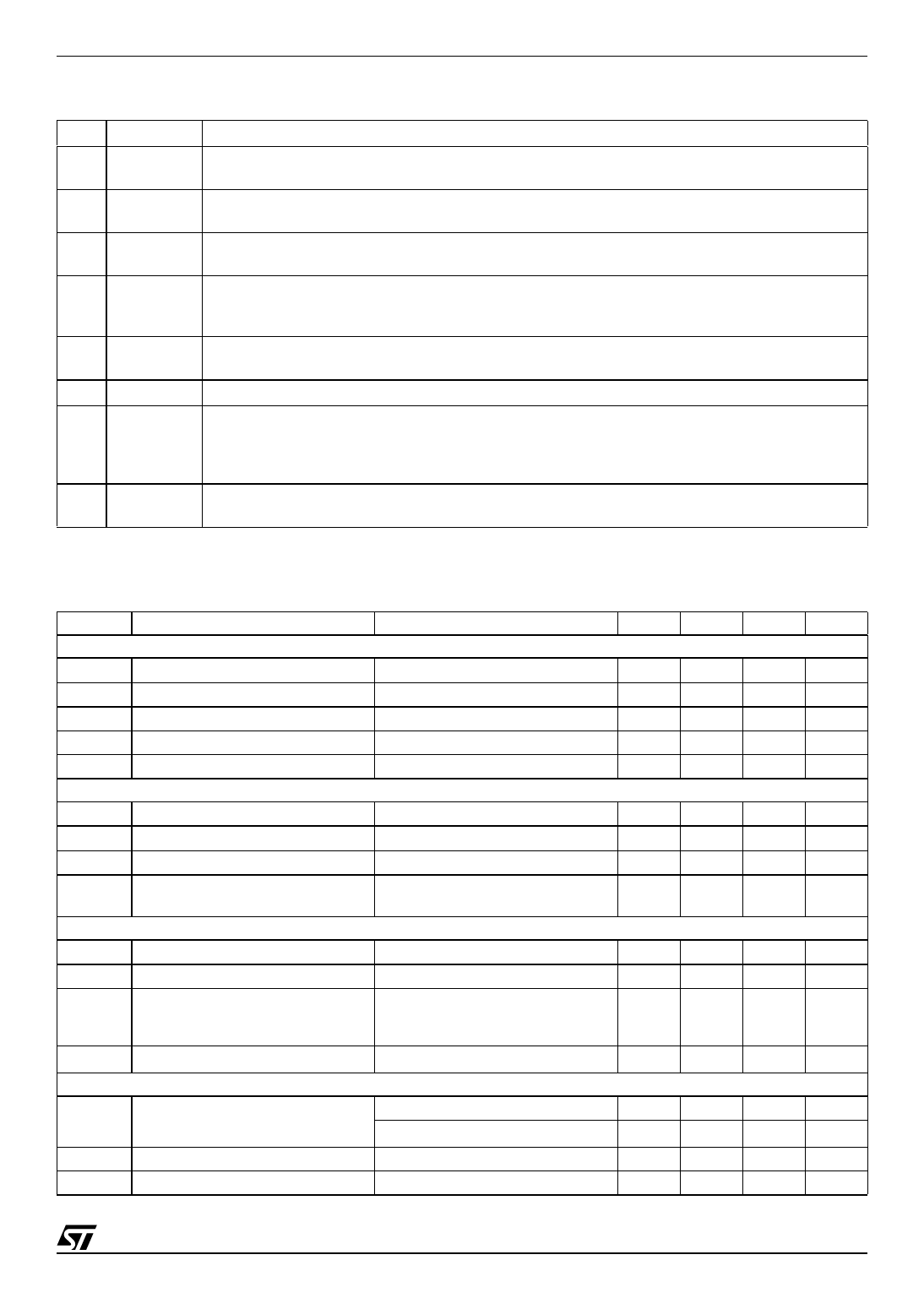
Table 4. Pin Description
N°
Pin
Function
1
INV
Inverting input of the error amplifier. The information on the output voltage of the PFC pre-
regulator is fed into the pin through a resistor divider.
2
COMP Output of the error amplifier. A compensation network is placed between this pin and INV (pin
#1) to achieve stability of the voltage control loop and ensure high power factor and low THD.
3
MULT Main input to the multiplier. This pin is connected to the rectified mains voltage via a resistor
divider and provides the sinusoidal reference to the current loop.
4
CS
Input to the PWM comparator. The current flowing in the MOSFET is sensed through a resistor,
the resulting voltage is applied to this pin and compared with an internal sinusoidal-shaped
reference, generated by the multiplier, to determine MOSFET’s turn-off.
5
ZCD Boost inductor’s demagnetization sensing input for transition-mode operation. A negative-going
edge triggers MOSFET’s turn-on.
6
GND Ground. Current return for both the signal part of the IC and the gate driver.
7
GD
Gate driver output. The totem pole output stage is able to drive power MOSFET’s and IGBT’s
with a peak current of 600 mA source and 800 mA sink. The high-level voltage of this pin is
clamped at about 12V to avoid excessive gate voltages in case the pin is supplied with a high
Vcc.
8
Vcc
Supply Voltage of both the signal part of the IC and the gate driver. The supply voltage upper
limit is extended to 22V min. to provide more headroom for supply voltage changes.
Table 5. Electrical Characteristics
(Tj = -25 to 125°C, VCC = 12, CO = 1 nF; unless otherwise specified)
Symbol
Parameter
SUPPLY VOLTAGE
VCC Operating range
VCCon Turn-on threshold
VCCOff Turn-off threshold
Hys Hysteresis
VZ Zener Voltage
SUPPLY CURRENT
Istart-up Start-up Current
Iq Quiescent Current
ICC Operating Supply Current
Iq
Quiescent Current
MULTIPLIER INPUT
IMULT Input Bias Current
VMULT Linear Operation Range
----∆----V----C----S----- Output Max. Slope
∆VMUL T
Test Condition
After turn-on
(1)
(1)
ICC = 20 mA
Before turn-on, VCC =11V
After turn-on
@ 70 kHz
During OVP (either static or
dynamic) or VZCD =150 mV
VVFF = 0 to 4 V
VMULT = 0 to 0.5V
VCOMP = Upper clamp
K
Gain (2)
ERROR AMPLIFIER
VINV Voltage Feedback Input
Threshold
Line Regulation
IINV Input Bias Current
VMULT = 1 V, VCOMP = 4 V
Tj = 25 °C
10.3 V < Vcc < 22 V (1)
Vcc = 10.3 V to 22V
VINV = 0 to 3 V
Min. Typ. Max. Unit
10.3
22
V
11
12
13
V
8.7
9.5 10.3
V
2.2
2.8
V
22
25
28
V
40
70
µA
2.5 3.75 mA
3.5
5
mA
2.2
mA
-1
µA
0 to 3
V
1.65 1.9
V/V
0.5
0.6
0.7
1/V
2.465 2.5 2.535 V
2.44
2.56
2
5
mV
-1
µA
3/16
Share Link: 