L6562D Ver la hoja de datos (PDF) - STMicroelectronics
Número de pieza
componentes Descripción
Fabricante
L6562D Datasheet PDF : 16 Pages
| |||
L6562
2 Description (continued)
The highly linear multiplier includes a special circuit, able to reduce AC input current distortion, that allows
wide-range-mains operation with an extremely low THD, even over a large load range.
The output voltage is controlled by means of a voltage-mode error amplifier and a precise (1% @Tj =
25°C) internal voltage reference.
The device features extremely low consumption (≤70 µA before start-up and <4 mA running) and includes
a disable function suitable for IC remote ON/OFF, which makes it easier to comply with energy saving
norms (Blue Angel, EnergyStar, Energy2000, etc.).
An effective two-step OVP enables to safely handle overvoltages either occurring at start-up or resulting
from load disconnection.
The totem-pole output stage, capable of 600 mA source and 800 mA sink current, is suitable for big MOS-
FET or IGBT drive which, combined with the other features, makes the device an excellent low-cost solu-
tion for EN61000-3-2 compliant SMPS's up to 300W.
Table 2. Absolute Maximum Ratings
Symbol
Pin
Parameter
VCC
8 IC Supply voltage (Icc = 20 mA)
---
1 to 4 Analog Inputs & Outputs
IZCD
5 Zero Current Detector Max. Current
Ptot
Power Dissipation @Tamb = 50°C
(DIP-8)
(SO-8)
Tj
Junction Temperature Operating range
Tstg
Storage Temperature
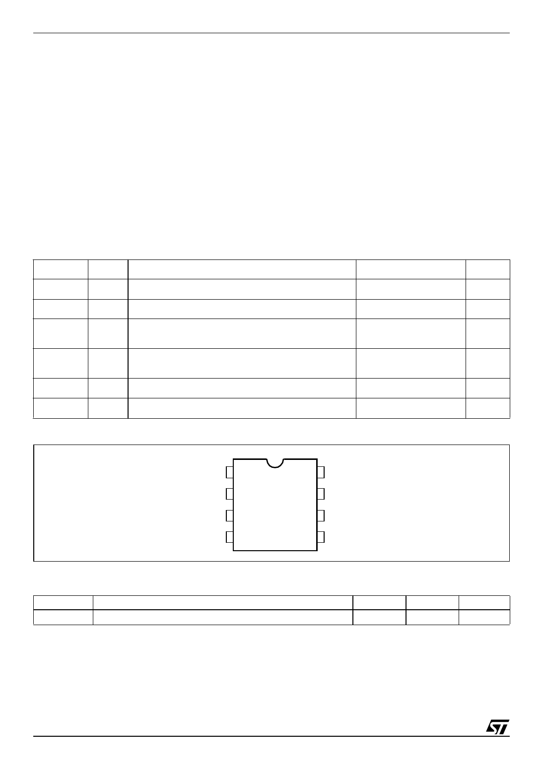
Figure 3. Pin Connection (Top view)
Value
Unit
self-limited
V
-0.3 to 8
V
-50 (source)
mA
10 (sink)
1
W
0.65
-40 to 150
°C
-55 to 150
°C
INV 1
COMP 2
MULT 3
CS 4
8 Vcc
7 GD
6 GND
5 ZCD
Table 3. Thermal Data
Symbol
Rth j-amb
Parameter
Max. Thermal Resistance, Junction-to-ambient
SO8
150
Minidip
100
Unit
°C/W
2/16
Share Link: 