L6562AT Ver la hoja de datos (PDF) - STMicroelectronics
Número de pieza
componentes Descripción
Fabricante
L6562AT Datasheet PDF : 25 Pages
| |||
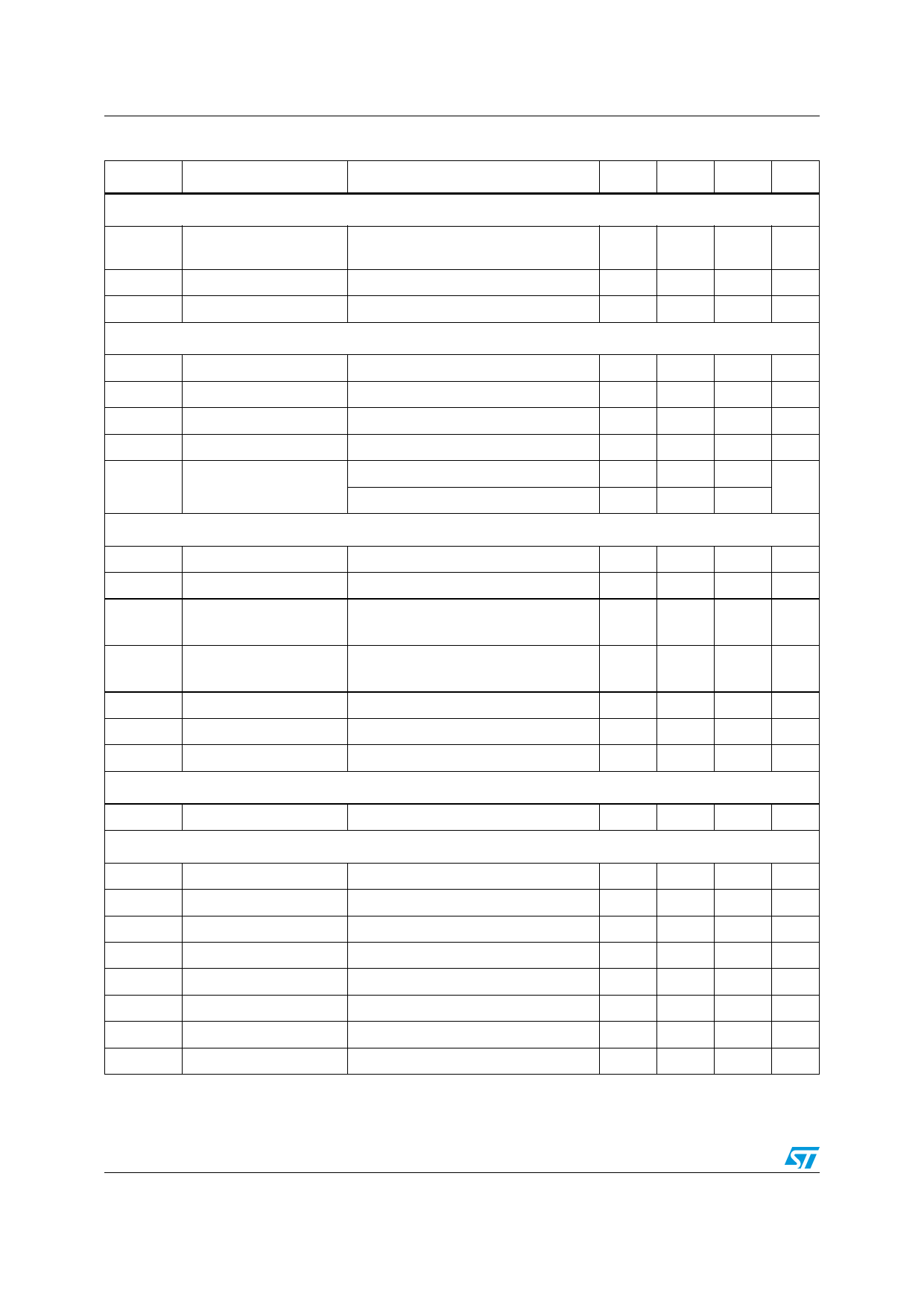
Electrical characteristics
L6562AT
Table 5. Electrical characteristics (continued)
Symbol
Parameter
Test condition
Output overvoltage
IOVP
Dynamic OVP triggering
current
Hys Hysteresis
(3)
Static OVP threshold
(1)
Current sense comparator
ICS
tLEB
td(H-L)
VCS
Input bias current
Leading edge blanking
Delay to output
Current sense clamp
Vcsoffset Current sense offset
Zero current detector
VCS = 0
VCOMP = Upper clamp, Vmult = 1.5 V
VMULT = 0
VMULT = 2.5 V
VZCDH
VZCDL
VZCDA
VZCDT
IZCDb
IZCDsrc
IZCDsnk
Starter
Upper clamp voltage
Lower clamp voltage
Arming voltage
(positive-going edge)
IZCD = 2.5 mA
IZCD = - 2.5 mA
(3)
Triggering voltage
(3)
(negative-going edge)
Input bias current
VZCD = 1 to 4.5 V
Source current capability
Sink current capability
tSTART Start timer period
Gate driver
VOL Output low voltage
Isink = 100 mA
VOH Output high voltage
Isource = 5 mA
Isrcpk Peak source current
Isnkpk Peak sink current
tf
Voltage fall time
tr
Voltage rise time
VOclamp Output clamp voltage
Isource = 5 mA; Vcc = 20 V
UVLO saturation
Vcc = 0 to VCCon, Isink = 2 mA
1. All the parameters are in tracking
( ) 2. The multiplier output is given by: Vcs = K ⋅ VMULT ⋅ VCOMP − 2.5
3. Parameters guaranteed by design, functionality tested in production.
7/25
Min Typ Max Unit
19.5
27
30.5 µA
20
µA
2.1 2.25 2.4
V
-1
µA
100 200 300 ns
175
ns
1.0 1.08 1.16 V
25
mV
5
5.0
5.7
6.5
V
-0.5
0
0.5
V
1.4
V
0.7
V
2
µA
-1.5
mA
1.5
mA
75
190 300 µs
0.6
1.2
V
9.5 10.3
V
-0.6
A
0.8
A
30
70
ns
60
130 ns
10
12
15
V
1.1
V
Share Link: 