L6229 Ver la hoja de datos (PDF) - STMicroelectronics
Número de pieza
componentes Descripción
Fabricante
L6229 Datasheet PDF : 25 Pages
| |||
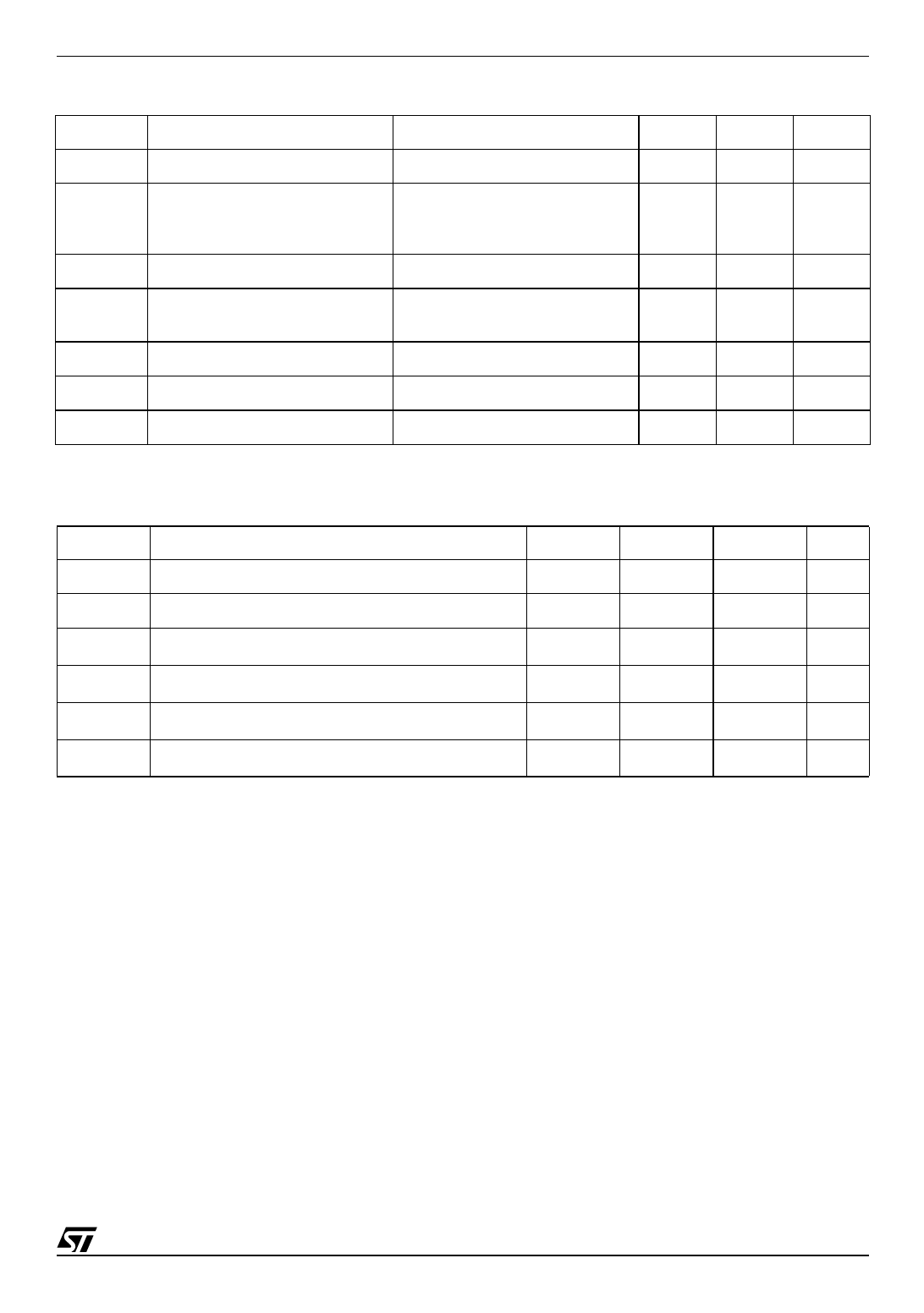
Table 3. Recommended Operating Condition
Symbol
Parameter
Test Conditions
VS
Supply Voltage
VSA = VSB = VS
VOD
Differential Voltage between:
VSA = VSB = VS;
VSA, OUT1, OUT2, SENSEA and VSENSEA = VSENSEB
VSB, OUT3, SENSEB
VREF Voltage Range at pin VREF
VSENSE Voltage Range at pins SENSEA
and SENSEB
(pulsed tW < trr)
(DC)
IOUT
DC Output Current
VSA = VSB = VS
TJ
Operating Junction Temperature
fSW
Switching Frequency
L6229
MIN
MAX
Unit
12
52
V
52
V
-0.1
5
V
-6
6
V
-1
1
V
1.4
A
-25
125
°C
100
KHz
Table 4. Thermal Data
Symbol
Description
PDIP24
SO24 PowerSO36 Unit
Rth(j-pins) Maximum Thermal Resistance Junction-Pins
19
15
°C/W
Rth(j-case) Maximum Thermal Resistance Junction-Case
2
°C/W
Rth(j-amb)1 MaximumThermal Resistance Junction-Ambient (1)
44
55
-
°C/W
Rth(j-amb)1 Maximum Thermal Resistance Junction-Ambient (2)
-
-
36
°C/W
Rth(j-amb)1 MaximumThermal Resistance Junction-Ambient (3)
-
-
16
°C/W
Rth(j-amb)2 Maximum Thermal Resistance Junction-Ambient (4)
59
78
63
°C/W
(1) Mounted on a multi-layer FR4 PCB with a dissipating copper surface on the bottom side of 6 cm2 (with a thickness of 35 µm).
(2) Mounted on a multi-layer FR4 PCB with a dissipating copper surface on the top side of 6 cm2 (with a thickness of 35 µm).
(3) Mounted on a multi-layer FR4 PCB with a dissipating copper surface on the top side of 6 cm2 (with a thickness of 35 µm),
16 via holes and a ground layer.
(4) Mounted on a multi-layer FR4 PCB without any heat-sinking surface on the board.
3/25
Share Link: 