L5994 Ver la hoja de datos (PDF) - STMicroelectronics
Número de pieza
componentes Descripción
Fabricante
L5994 Datasheet PDF : 26 Pages
| |||
L5994 - L5994A
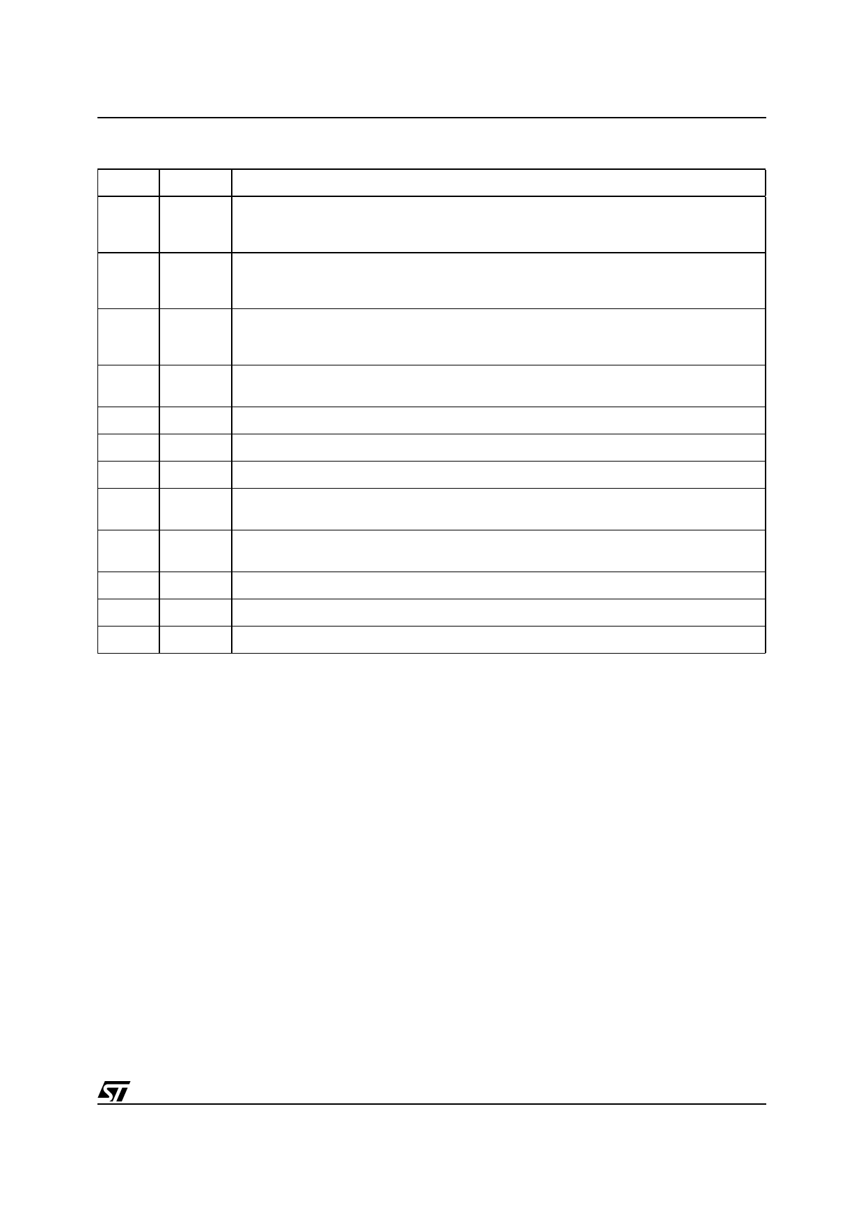
PIN DESCRIPTION (continued)
N°
Name
Function
21
VDRLIN Linear regulator driver connection. It must be connected to the base pin of an external PNP
transistor and, through a resistor, to its emitter in order to supply the internal driver.
If no linear regulation is implemented, it may be left floating.
22
VFBLIN Feedback input for the linear regulator. It must be connected directly, or through a resistor
divider, to the linear regulated output. If no linear regulation is implemented, it may be left
floating
23
PWROK2 Power Good open drain diagnostic signal. This output is in high inpedence when sect. 2 is
enabled and running properly after a delay defined by the CRST capacitor. When not used
may be left floating.
24 H2STRAP Section 2 bootstrap capacitor connection. A bootstrap capacitor must be connected between
this pin and pin H2SRC to supply the H2GATE driver.
25
H2GATE Gate driver for the section 2, high side NMOS
26
H2SRC Section 2 High side NMOS source connection.
27
R2GATE Gate driver for the section 2, low side NMOS (synchronuos rectifier)
28
PGND Current return for power mosfet driver for both sections. Connect to the low side mosfet
sources pin. It must be routed separately from signal current returns
29
PREG5 5V internal regulator output. Used mainly to supply the bootstrap capacitors and the internal
circuitry connected to SREG5 via a low-pass filter.
30
R1GATE Gate driver for the section 1, low side NMOS (synchronuos rectifier)
31
H1SRC Section 1 High side NMOS source connection.
32
H1GATE Gate driver for the section 1, high side NMOS
Detailed Functional Description
In the device block diagram six fundamental functional blocks can be identified:
· 1.9V to 5.1V step-down PWM switching regulator (section 1, pins 1, 4 to 8, 30 to 32);
· 1.66V to 3.3V step-down PWM switching regulator (section 2, pins 17 to 20, 24 to 27);
· Linear regulator driver for an external PNP transistor (pins 21,22);
· 5V low drop-out linear regulator (pin 29);
· 2.5V reference voltage generator (pin 12);
· Power Management section (pins 9 to 11, 14,16).
The chip is supplied through pin Vin (2), typically by a battery pack or the output of an AC-DC adapter, with a
voltage that can range from 5V to 25V. The return of the bias current of the device is the signal ground pin SGND
(13), which references the internal logic circuitry. The drivers of the external MOSFET's have their separate cur-
rent return, namely the power ground pin PGND (28). Take care of keeping separate the routes of signal ground
and the power ground pin when laying out the PCB (see "Layout and grounding" section). The two PWM regu-
lators share the internal oscillator, programmable or synchronizable through pin OSC (15).
PWM Regulators
Each PWM regulator includes control circuitry as well as gate-drive circuits for a step-down DC-DC converter
in buck topology using synchronous rectification and current mode control.
The two regulators are independent and almost identical. As one can see in the Block Diagram, they share only
7/26
Share Link: 