L4973D3.3-L4973D5.1 Ver la hoja de datos (PDF) - STMicroelectronics
Número de pieza
componentes Descripción
Fabricante
L4973D3.3-L4973D5.1 Datasheet PDF : 16 Pages
| |||
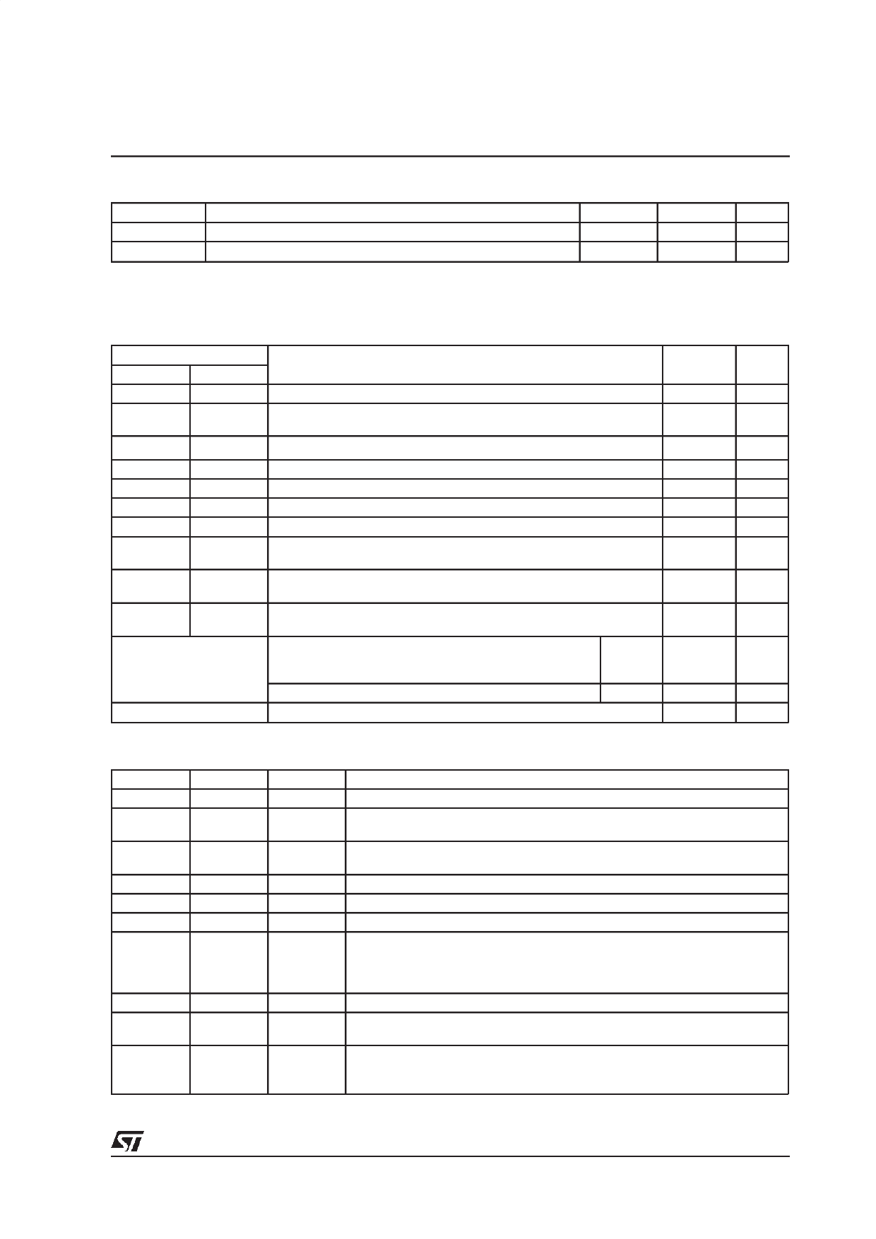
THERMAL DATA
Symbol
Rth(j-pin)
Rth(j-amb)
Parameter
Thermal Resistance Junction to pin
Thermal Resistance to Ambient
(*) Package mounted on board.
L4973V3 - L4973V5 - L4973D3 - L4973D5
Max.
Max.
Powerdip
12
60 (*)
SO20
15
80 (*)
Unit
°C/W
°C/W
ABSOLUTE MAXIMUM RATINGS
Symbol
DIP-18
S0-20
V7,V8
V9,V8
V2,V3
V2,V3
I2,I3
V9-V8
V9
V1 1
V17
V12
I2,I3
V10-V8
V10
V12
V19
V13
Parameter
Input voltage
Output DC voltage
Output peak voltage at t = 0.1µs f=200KHz
Maximum output current
Bootstrap voltage
Analogs input voltage (VCC = 24V)
Analogs input voltage (VCC = 24V)
(VCC = 20V)
V18
V20
(VCC = 20V)
V10
V11
Inhibit
Ptot
TJ,TSTG
Power dissipation a Tpins ≤ 90°C
(Tamb = 70°C no copper area)
(Tamb = 70°C 4cm copper area on PCB)
Power dissipation a Tpins = 90°C
Junction and storage temperature
Value
Unit
58
V
-1
V
-5
V
int. limit.
14
V
70
V
12
V
13
V
6
V
-0.3
V
5.5
V
-0.3
V
Vcc
V
-0.3
V
DIP
5
W
12+3+3
1.3
W
2
W
SO20
4
W
-40 to 150 °C
PIN FUNCTIONS
Powerdip
11
10
SO20
12
11
9
10
18
20
7,8
8,9
2,3
2,3
12
13
16
4,5,6
13,14,15
1
18
4,5,6,7
14,15,16,17
1
NAME
COMP
INH
BOOT
SYNC
Vcc
OUT
VFB
V5.1
GND
OSC
DESCRIPTION
E/A output to be used for frequency compensation
A logic signal (active high) disables the device (sleep mode operation).
If not used it must be connected to GND; if floating the device is disabled.
A capacitor connected between this pin and the output allows to drive the
internal D-MOS.
Input/Output synchronization.
Unregulated DC input voltage
Stepdown regulator output.
Stepdown feedback input. Connecting the output directly to this pin results
in an output voltage of 3.3V for the L4973V3.3 and 5.1V. An external
resistive divider is required for higher output voltages. For output voltage
less than 3.3V, see note ** and Figure 32.
Reference voltage externally available.
Signal ground
An external resistor connected between the unregulated input voltage and
Pin 1 and a capacitor connected from Pin 1 to ground fixes the switching
frequency. (Line feed forward is automatically obtained)
3/16
Share Link: 