SAA7165WP Ver la hoja de datos (PDF) - Philips Electronics
Número de pieza
componentes Descripción
Fabricante
SAA7165WP Datasheet PDF : 28 Pages
| |||

Philips Semiconductors
Video Enhancement and Digital-to-Analog
processor (VEDA2)
Product specification
SAA7165
Interpolation
The chrominance interpolation filter consists of various
filter stages, multiplexers and de-multiplexers to increase
the data rate of the colour-difference signals by a factor of
2 or 4. The switching of the filters by the bits IFF, IFC and
IFL is described previously. Additional signal samples with
significant amplitudes between two consecutive signal
samples of the low data rate are generated.
The time-multiplexed U and V samples are stored in
parallel for converting.
Data switch
The digital signals are adapted to the conversation range.
U and V data have 8-bit formats again; Y can have 9 bits
dependent on peaking. Blanking and switching to
colourless level is applied here. Bits can be inverted by
INV-bit to change the polarity of colour-difference output
signals.
Digital Colour Transient Improvement (DCTI)
The DCTI circuit improves the transition behaviour of the
UV colour-difference signals. As the CVBS signal allows
for a 4 : 1 : 1 bandwidth representation only, the DCTI
improves the transients to the same performance as
signals coming from a 4 : 2 : 2 source, or even more.
In order to obtain the point of inflection, the second
derivative of the signal is calculated. The improved
transition is centred with respect to the point of inflection of
the original signal. Thus, there is no horizontal shift of the
resulting signal.
The transition area length to be improved is controlled via
I2C-bus by the bits LI1 and LI0 (Table 5); the sensitivity of
the DCTI block is controlled by the bits GA1 and GA0.
The CMO bit controls the colour detail sensitivity. It should
be set to logic 1 (ON) if the video signal contains fine
colour details (recommended operation mode).
Digital-to-Analog Converters (DACs)
Conversion is separate for Y, U and V. The converters use
resistor chains with low-impedance output buffers.
The minimum output voltage is 200 mV to reduce integral
non-linearity errors. The analog signal, without load on
output pin, is between 0.2 and 2.2 V floating.
An application for 1 V/75 Ω on outputs is shown in Fig.14.
Each digital-to-analog converter has its own supply and
ground pins suitable for decoupling. The reference
voltage, supplying the resistor chain of all three DACs, is
the supply voltage VDDA4. The current into pin 41 is
0.3 mA; a larger current improves the bandwidth but
increases the integral non-linearity.
I2C-bus format
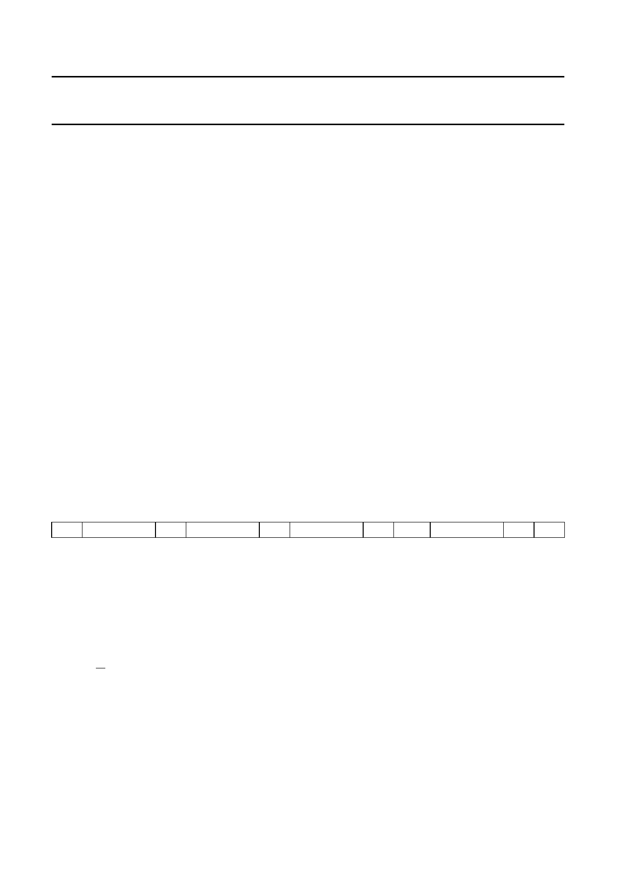
Table 4 I2C-bus format; see notes 1 to 7
S slave address A subaddress A data 0
A
... data n
AP
Notes
1. S = START condition.
2. Slave address = 1011 111X.
3. A = acknowledge; generated by the slave.
4. Subaddress = subaddress byte (Table 5);
If more than 1 byte of DATA is transmitted, then auto-increment of the subaddress is performed.
5. Data = data byte (Table 5).
6. P = STOP condition.
7. X = R/W control bit:
a) X = 0; order to write (the circuit is slave receiver).
b) X = 1; order to read (the circuit is slave transmitter).
1996 Aug 20
9