PCF84C41A Ver la hoja de datos (PDF) - Philips Electronics
Número de pieza
componentes Descripción
Fabricante
PCF84C41A Datasheet PDF : 20 Pages
| |||
Philips Semiconductors
Telecom microcontrollers
Product specification
PCF84C21A; PCF84C41A;
PCF84C81A
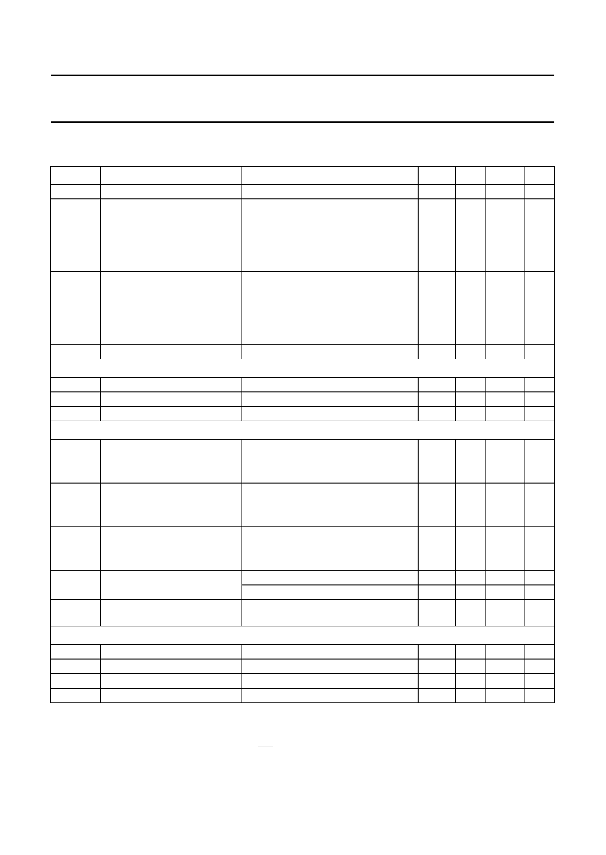
11 DC CHARACTERISTICS
VDD = 2.5 to 5.5 V; VSS = 0 V; Tamb = −40 to +85 °C; all voltages with respect to VSS; unless otherwise specified.
SYMBOL
PARAMETER
CONDITIONS
MIN. TYP. MAX. UNIT
VDD
operating supply voltage
see Fig.3
2.5
−
5.5
V
IDD
operating supply current
note 1; see Figs 4 and 5
VDD = 3 V; fxtal = 3.58 MHz (gmL)
−
0.3 0.6
mA
VDD = 5 V; fxtal = 10 MHz (gmL)
−
1.1 3.0
mA
VDD = 5 V; fxtal = 16 MHz (gmM)
−
1.7 5.0
mA
VDD = 5 V; fxtal = 16 MHz (gmH)
−
2.5 6.0
mA
IDD(idle) supply current (Idle mode)
note 1; see Figs 6 and 7
VDD = 3 V; fxtal = 3.58 MHz (gmL)
−
0.2 0.4
mA
VDD = 5 V; fxtal = 10 MHz (gmL)
−
0.8 1.6
mA
VDD = 5 V; fxtal = 16 MHz (gmM)
−
1.2 4.0
mA
VDD = 5 V; fxtal = 16 MHz (gmH)
−
1.7 5.0
mA
IDD(stp) supply current (Stop mode)
VDD = 2.5 V; notes 1 and 2; see Fig.8 −
1.2 10
µA
Inputs
VIL
LOW level input voltage
VIH
HIGH level input voltage
ILI
input leakage
VSS ≤ VI ≤ VDD
0
−
0.7VDD −
−1
−
0.3VDD V
VDD
V
+1
µA
Outputs
IOL
LOW level output sink current VDD = 5 V; VO = 0.4 V; see Fig.9
[except Port 1; SDA/P2.3 and
PCF84C21A; PCF84C41A
SCLK]
PCF84C81A
1.6
12 −
mA
1.6
5
−
mA
IOL1
LOW level output sink current; VDD = 5 V; VO = 1.2 V; see Fig.10
Port 1
PCF84C21A; PCF84C41A
10
30 −
mA
PCF84C81A
10
19 −
mA
IOL2
LOW level output sink current; VDD = 5 V; VO = 0.4 V; see Fig.11
SDA/P2.3 and SCLK
PCF84C21A; PCF84C41A
3
12 −
mA
PCF84C81A
3
6.5 −
mA
IOH
HIGH level pull-up output
VDD = 5 V; VO = 3.5 V; see Fig.12
40
100 −
µA
source current
VDD = 5 V; VO = 0 V; see Fig.12
−
−140 −400 µA
IOH1
HIGH level push-pull output
VDD = 5 V; VO = 4.6 V; see Fig.13
−1.6 −7 −
mA
source current
Oscillator (see Fig.14)
gmL
LOW transconductance
VDD = 5 V
0.2
0.4 1.0
mS
gmM
MEDIUM transconductance
VDD = 5 V
0.9
1.6 3.2
mS
gmH
HIGH transconductance
RF
feedback resistor
VDD = 5 V
3.0
4.5 9.0
mS
0.3
1.0 3.0
MΩ
Notes
1. VIL = VSS; VIH = VDD; open drain outputs connected to VSS; all other outputs, including XTAL2, open (typical values
at 25 °C with crystal connected between XTAL1 and XTAL2).
2. VIL = VSS; VIH = VDD; RESET and T1 at VSS; INT/T0 at VDD; crystal connected between XTAL1 and XTAL2; open
drain outputs connected to VSS; all other outputs open.
1996 Nov 20
7
Share Link: 