PCF84C41A Ver la hoja de datos (PDF) - Philips Electronics
Número de pieza
componentes Descripción
Fabricante
PCF84C41A Datasheet PDF : 20 Pages
| |||
Philips Semiconductors
Telecom microcontrollers
Product specification
PCF84C21A; PCF84C41A;
PCF84C81A
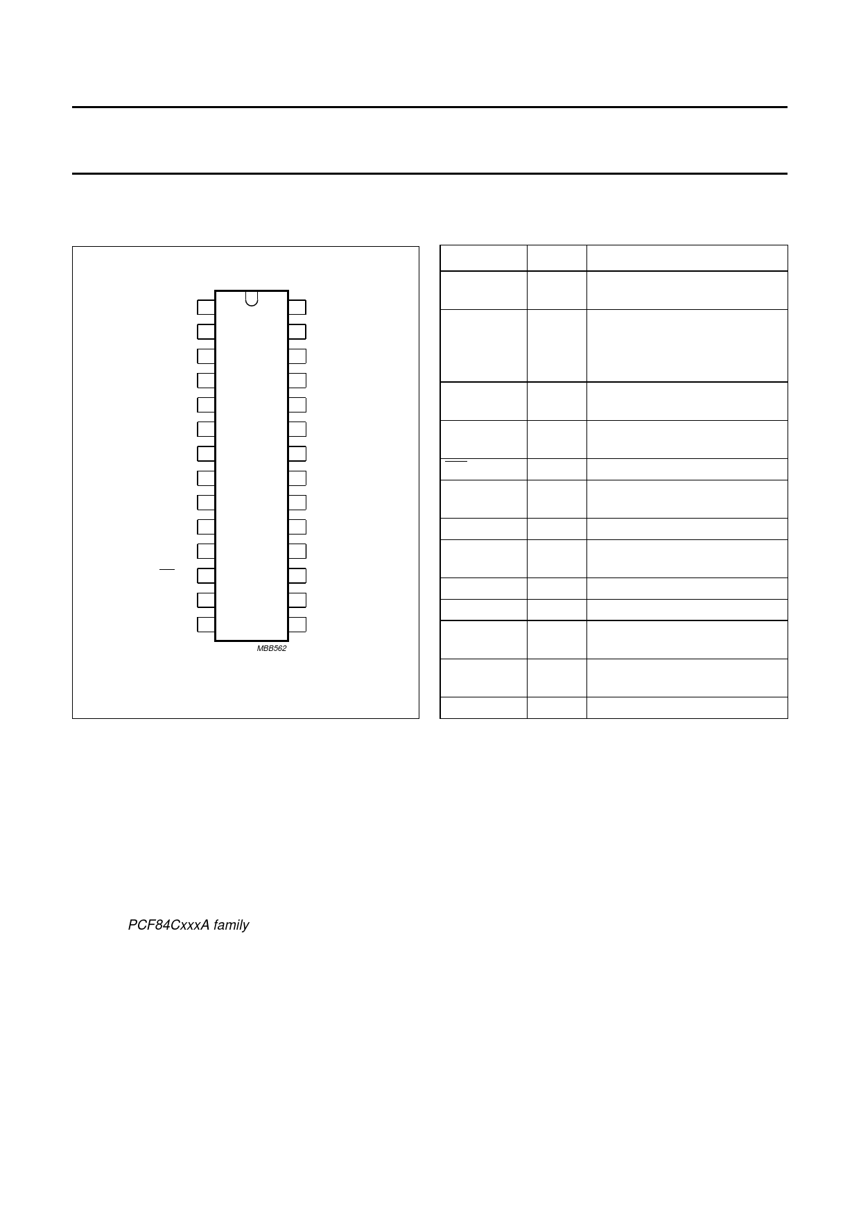
5 PINNING INFORMATION
5.1 Pinning
P2.2 1
SDA/P2.3 2
28 V DD
27 P2.1
SCLK 3
26 P2.0
P0.0 4
25 P1.7
P0.1 5
24 P1.6
P0.2 6
23 P1.5
P0.3 7 PCF84C21A 22 P1.4
PCF84C41A
P0.4 8 PCF84C81A 21 P1.3
P0.5 9
20 P1.2
P0.6 10
19 P1.1
P0.7 11
18 P1.0
INT/T0 12
17 RESET
T1 13
VSS 14
16 XTAL2
15 XTAL1
MBB562
Fig.2 Pin configuration.
5.2 Pin description
Table 1 DIP28 and SO28 packages
SYMBOL PIN
FUNCTION
P2.2
1
1 bit of Port 2: 4-bit
quasi-bidirectional I/O port
SDA/P2.3 2
bidirectional data line of the
I2C-bus interface, or 1 bit of
Port 2: 4-bit quasi-bidirectional
I/O port
SCLK
3
bidirectional clock line of the
I2C-bus interface
P0.0 to P0.7 4 to 11 8 bits of Port 0: 8-bit
quasi-bidirectional I/O port
INT/T0
12
Interrupt/Test 0
T1
13
Test 1/count input of 8-bit
timer/event counter 1
VSS
14
ground
XTAL1
15
crystal oscillator input or
external clock input
XTAL2
16
crystal oscillator output
RESET
17
Reset input
P1.0 to P1.7 18 to 25 8 bits of Port 1: 8-bit
quasi-bidirectional I/O port
P2.0 to P2.1 26 to 27 2 bits of Port 2: 4-bit
quasi-bidirectional I/O port
VDD
28
positive supply
6 INSTRUCTION SET
ROM is restricted to 2 kbytes for the PCF84C21A and
4 kbytes for the PCF84C41A. Therefore, the instructions
SEL MB1/2/3 for the PCF84C21A, and the instructions
SEL MB2/3 for the PCF84C41A should be avoided, as
they would define non-existing program memory banks.
As RAM is limited to 64 bytes for the PCF84C21A and to
128 bytes for the PCF84C41A, care should be taken to
avoid accesses to non-existing RAM locations.
See the “PCF84CxxxA family” data sheet for a complete
description of the instruction set.
7 HIGH SINK OUTPUT CURRENTS
The Port 1 outputs of these devices are designed for high
current drive in the logic 0 state. They are capable of
driving 10 mA loads and higher. Applications include drive
for small relays and light-emitting diodes (LEDs).
To avoid overload, care should be taken that the total
Port 1 current averages less than 80 mA, i.e. an average
of 10 mA per Port 1 line. Refer to Chapter “Limiting values”
which specifies an upper limit of 100 mA for ISS.
1996 Nov 20
5
Share Link: 