KA3882E Ver la hoja de datos (PDF) - Fairchild Semiconductor
Número de pieza
componentes Descripción
Fabricante
KA3882E Datasheet PDF : 6 Pages
| |||
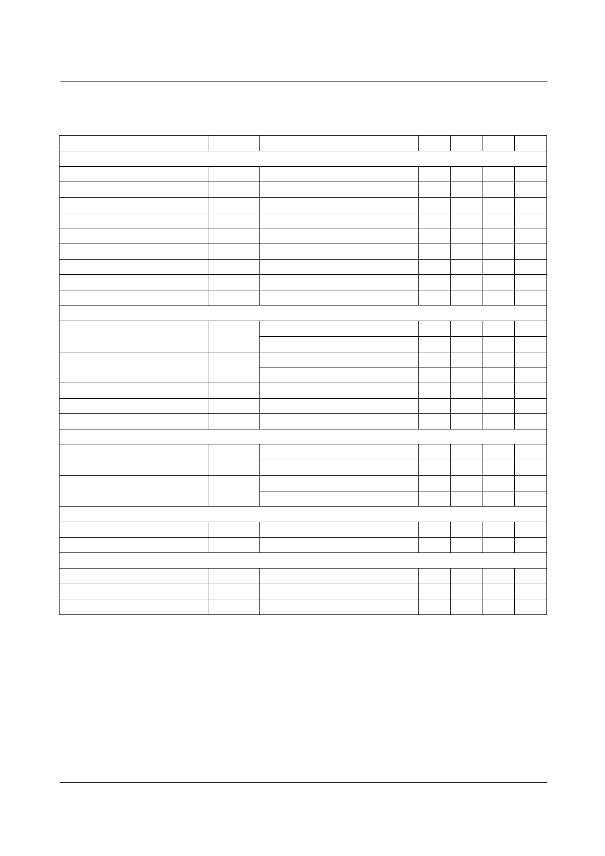
KA3882E/KA3883E
Electrical Characteristics (Continued)
(VCC = 15V, RT = 10kΩ, CT = 3.3nF, TA = 0°C to +70°C, Unless otherwise specified)
Parameter
ERROR AMPLIFIER SECTION
Input voltage
Input bias current
Open loop gain
Unity gain bandwidth
PSRR
Output sink current
Output source current
Output high voltage
Output low voltage
OUTPUT SECTION
Symbol
VI
IBIAS
GVO
GBW
PSRR
ISINK
ISOURCE
VOH
VOL
Output low level
VOL
Output high level
VOH
Rise time
tR
Fall time
tF
Output voltage swing limit
VOLIM
UNDER VOLTAGE LOCKOUT SECTION
Start threshold
VTH
Min. operating voltage
( after turn on )
PWM SECTION
Maximum duty cycle
Minimum duty cycle
TOTAL STANDBY CURRENT
Start-up current
Operating supply current
VCC zener voltage
VTL
DMAX
DMIN
IST
ICC
VZ
Conditions
VPIN1 = 2.5V
VFB=0V
VO = 2V to 4V (Note1)
TJ= 25°C (Note1)
VCC = 12V to 25V (Note1)
VPIN2 = 2.7V, VPIN1 = 1.1V
VPIN2 = 2.3V, VPIN1 = 5.0V
VPIN2 = 2.3V, R1 = 15kΩ to GND
VPIN2 = 2.7V, R1 = 15kΩ to Vref
ISINK = 20mA
ISINK = 200mA
ISOURCE = 20mA
ISOURCE = 200mA
TJ = 25°C, C1 = 1nF (Note1)
TJ = 25°C, C1 = 1nF (Note1)
VCC = 27V, C1 = 1nF
KA3882E
KA3883E
KA3882E
KA3883E
KA3882E/KA3883E
-
-
VPIN2 = VPIN3 = 0V
ICC = 25mA
Min. Typ. Max. Unit
2.42 2.50 2.58 V
- -0.3 - 2 uA
65 90
-
dB
0.7 1
- MHz
60 70
-
dB
2
6
- mA
-0.5 -0.8 - mA
5
6
-
V
- 0.8 1.1 V
- 0.1 0.4 V
- 1.5 2.2 V
13 13.5 -
V
12 13.5 -
V
-
40 100 ns
-
40 100 ns
-
22
-
V
15 16 17 V
7.8 8.4 9.0 V
9 10 11 V
7.0 7.6 8.2 V
94 96 100 %
-
-
0
%
- 0.2 0.4 mA
-
11 17 mA
-
29
-
V
* Adjust VCC above the start threshold before setting at 15V
Notes :
1. These parameters, although guaranteed, are not 100% tested in production.
2. Parameter measured at trip point of latch with VFB = 0V.
3.
Gain defined as:
GV
=
--∆----V----C----O----M----P--
∆VSENSE
;0
≤
VSENSE
≤
0.8V
4. Junction-to-air thermal resistance test enviroments.
-. PCB information ;
Board thickness : 1.6mm , Board dimension : 76.2 X 114.3mm2 , Ref. : EIA / JSED51-3 and EIA / JSED51-7
-. Board structure; Using the single layer PCB.
3
Share Link: 