IXDD404 Ver la hoja de datos (PDF) - IXYS CORPORATION
Número de pieza
componentes Descripción
Fabricante
IXDD404 Datasheet PDF : 12 Pages
| |||
Pin Configurations
SO8 (SI)
8 PIN DIP (PI)
1 EN A
2 IN A
3 GND
4 IN B
I
EN B 8
X
D OUT A 7
D
4
VCC 6
0
4
OUT B 5
SO16 (SI-16)
IXDD404
Pin Description
SYMBOL
FUNCTION
EN A
A Channel Enable
IN A
A Channel Input
GND
Ground
IN B
OUT B
B Channel Input
B Channel Output
VCC
Supply Voltage
OUT A
A Channel Output
EN B
B Channel Enable
DESCRIPTION
The Channel A enable pin. This pin, when driven low, disables the A
Channel, forcing a high impedance state to the A Channel Output.
A Channel Input signal-TTL or CMOS compatible.
The system ground pin. Internally connected to all circuitry, this pin provides
ground reference for the entire chip. This pin should be connected to a low
noise analog ground plane for optimum performance.
B Channel Input signal-TTL or CMOS compatible.
B Channel Driver output. For application purposes, this pin is connected,
through a resistor, to Gate of a MOSFET/IGBT.
Positive power-supply voltage input. This pin provides power to the entire
chip. The range for this voltage is from 4.5V to 35V.
A Channel Driver output. For application purposes, this pin is connected,
through a resistor, to Gate of a MOSFET/IGBT.
The Channel B enable pin. This pin, when driven low, disables the B
Channel, forcing a high impedance state to the B Channel Output.
CAUTION: These devices are sensitive to electrostatic discharge; follow proper ESD procedures when
handling and assembling this component.
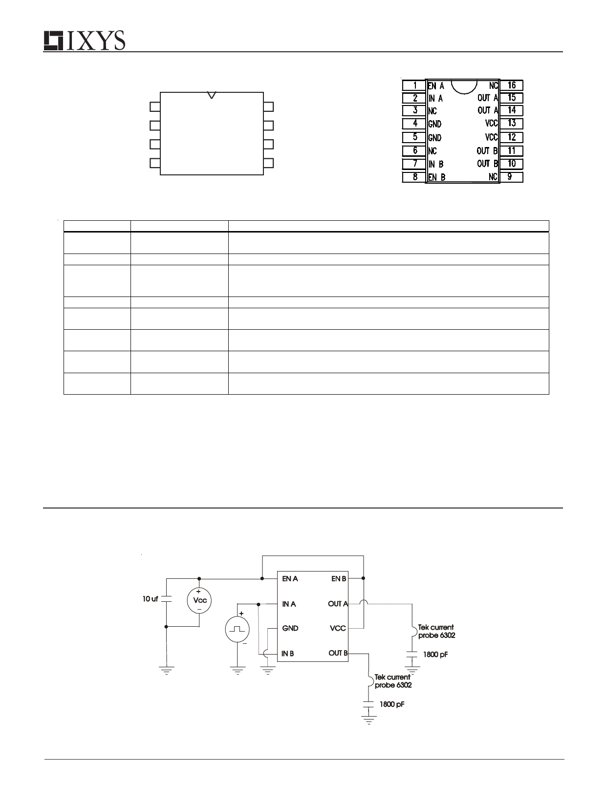
Figure 2 - Characteristics Test Diagram
VIN
4
Share Link: 