IXDP610 Ver la hoja de datos (PDF) - IXYS CORPORATION
Número de pieza
componentes Descripción
Fabricante
IXDP610 Datasheet PDF : 8 Pages
| |||
IXDP 610
Symbol
Definition
Operating Range
VCC
Supply voltage
TA
Operating free air temperature
Maximum Ratings
min. max.
4.5 5.5
V
-40 85
°C
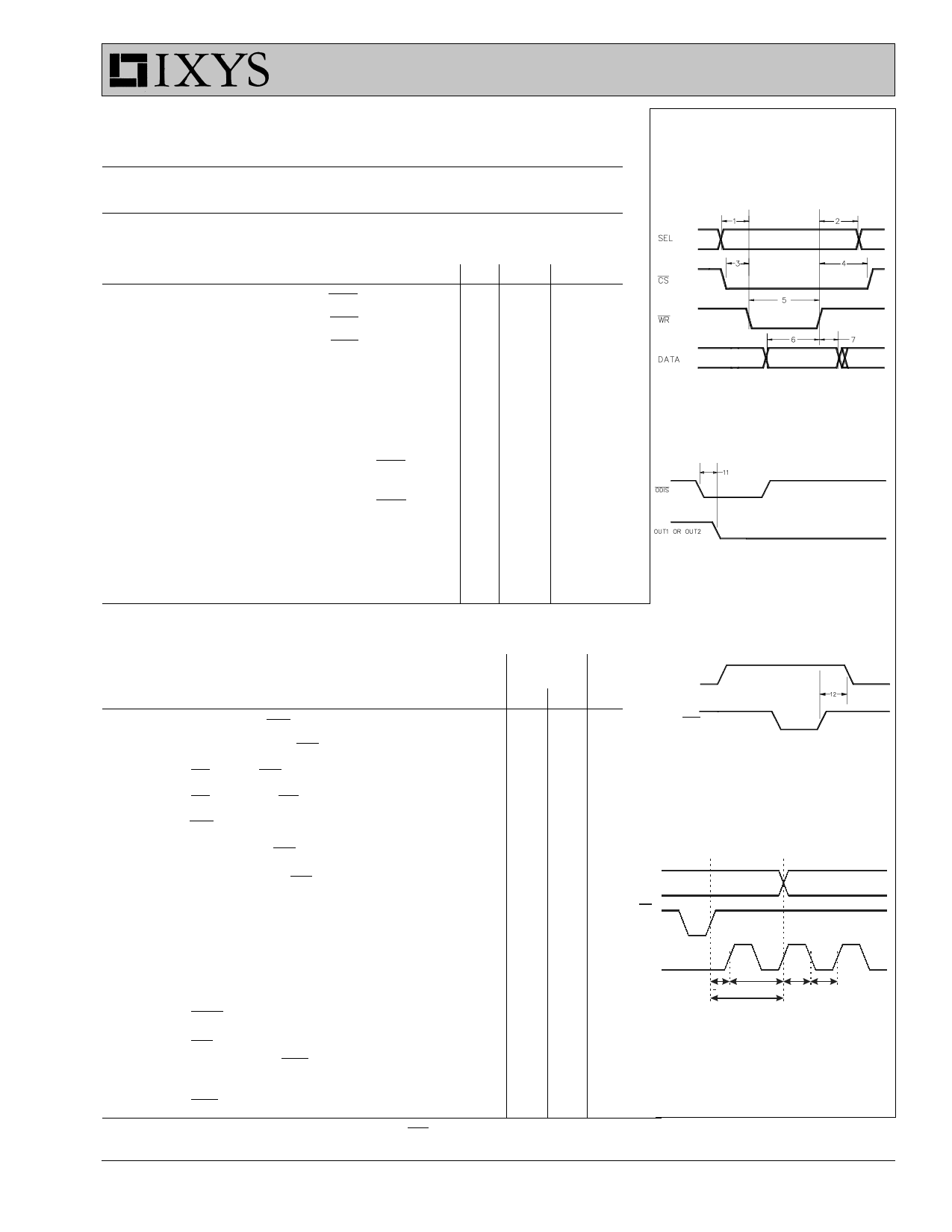
Numbers in the Fig. 3 to 6 corres-
ponding to the time values on the
bottom left of this page.
Symbol
Definition/Condition
Characteristic Values
(Over operating range, unless otherwise specified)
min. typ. max.
VIH(CMOS)
VIL(CMOS)
VH
VOH
VOL
VIH(TTL)
VIL(TTL)
ILI
ICC
Symbol
No. see
Fig. 3-6
Input High Voltage ODIS
3.8
Input Low Voltage ODIS
-0.3
Input Hysteresis
ODIS
0.3
Output High Voltage OUT1 IOH = -20 mA 2.4
OUT2
Output Low Voltage OUT1 IOL = 20 mA
OUT2
Input High Voltage All Inputs
2.0
Except ODIS
Input Low Voltage All Inputs
-0.3
Except ODIS
Input Leakage
All Inputs
-10
Current
0 < VI < VCC
Power Supply
Current
fCLK = 5 MHz
VIH = VCC or 0
VCC +0.3 V
1.2 V
0.5
V
V
0.4 V
VCC +0.3 V
0.8 V
-0.1 10 µA
3.5 10 mA
Definition/Condition
Characteristic Values
(TA = 25°C, VCC = 5 V ± 10 %, C1 = 50 pF)
-40...85°C
typ.
min. max.
Fig. 3 Write operation timing diagram
Fig. 4 Output disable to outputs off
timing
OUT 1 or OUT2
1
tAVWL
2 tWHAX
3 tSLWL
4 tWHSH
5 tWLWH
6 tDVWH
7 tWHDX
8 fCLK
9 tCLCH
tCHCL
10 tCHOV
SEL Stable to WR Low
SEL Stable after WR High
CS Low to WR Low
CS High after WR High
WR Pulse Width
8
Data Valid to WR High
Data Held after WR High
10
Clock Frequency
50*
Clock Pulse Duration Low 12.5
High 12.5
CLK to Output when
Writing to PW latch
5+½TCLK**
11 tODLOL
ODIS Low to Output Low
20
12 tWHOL
WR High to Output Low
30
When Writing Stop to the
Control latch
13 tRLRH
RST Low Time
* Output will change 1 rising CLOCK edge +5ns after WR (see Fig. 6)
** Tclk = 1/fclk
© 2001 IXYS/DEI All rights reserved
5
ns
10
ns
5
ns
5
ns
20
ns
5
ns
20
ns
0 50* MHz
12.5
ns
12.5
ns
5 5+TCLK ns
50
ns
60 ns
50
ns
WR
Fig. 5 Stop to outputs off timing
OUT1
OUT2
WR
CLK
1
2
3
<5ns
8
10
9
9
Fig. 6 CLOCK to output when writing
to PW latch
2
Share Link: 