IRU1150 Ver la hoja de datos (PDF) - International Rectifier
Número de pieza
componentes Descripción
Fabricante
IRU1150 Datasheet PDF : 9 Pages
| |||
IRU1150(PbF)
Note 1: Low duty cycle pulse testing with Kelvin con-
nections is required in order to maintain accurate data.
Note 2: Dropout voltage is defined as the minimum dif-
ferential between VIN and VOUT required to maintain regu-
lation at VOUT. It is measured when the output voltage
drops 1% below its nominal value.
Note 3: Minimum load current is defined as the mini-
mum current required at the output in order for the out-
put voltage to maintain regulation. Typically the resistor
dividers are selected such that it automatically main-
tains this current.
PIN DESCRIPTIONS
PIN # PIN SYMBOL PIN DESCRIPTION
1
VSENSE
This pin is the positive side of the reference which allows remote load sensing to achieve
excellent load regulation.
2
Adj
A resistor divider from this pin to the VOUT pin and ground sets the output voltage.
3
VOUT
The output of the regulator. A minimum of 10µF capacitor must be connected from this
pin to ground to insure stability.
4
VCTRL
This pin is the supply pin for the internal control circuitry as well as the base drive for the
pass transistor. This pin must always be higher than the VOUT pin in order for the device to
regulate. (See specifications)
5
VIN
The input pin of the regulator. Typically a large storage capacitor is connected from this
pin to ground to insure that the input voltage does not sag below the minimum drop out
voltage during the load transient response. This pin must always be higher than VOUT in
order for the device to regulate. (See specifications)
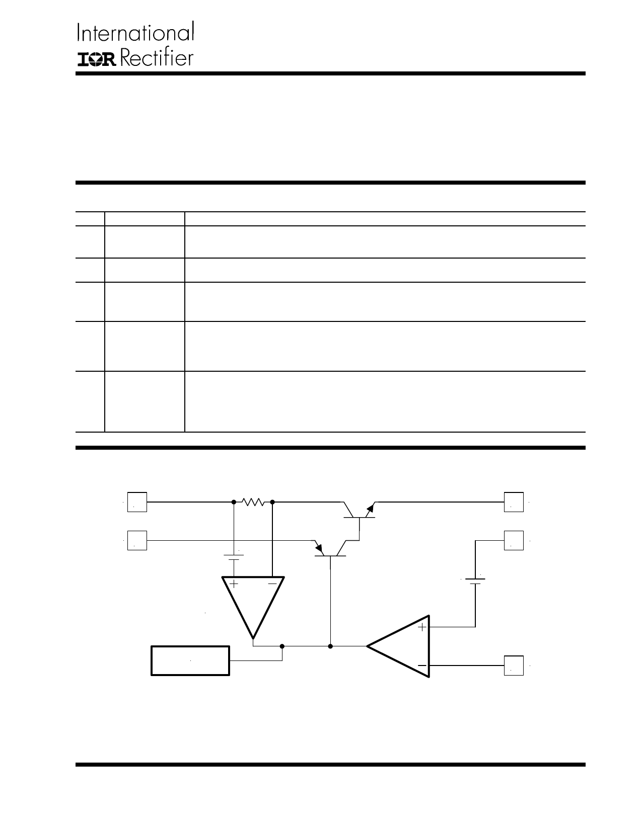
BLOCK DIAGRAM
VIN 5
VCTRL 4
+
CURRENT
LIMIT
THERMAL
SHUTDOWN
3 VOUT
1 VSENSE
1.25V +
2 Adj
Figure 2 - Simplified block diagram of the IRU1150.
Rev. 1.8
www.irf.com
3
Share Link: 