IS25F011A Ver la hoja de datos (PDF) - Integrated Silicon Solution
Número de pieza
componentes Descripción
Fabricante
IS25F011A
IS25F011A Datasheet PDF : 23 Pages
| |||

IS25F011A
IS25F021A
IS25F041A
ISSI ®
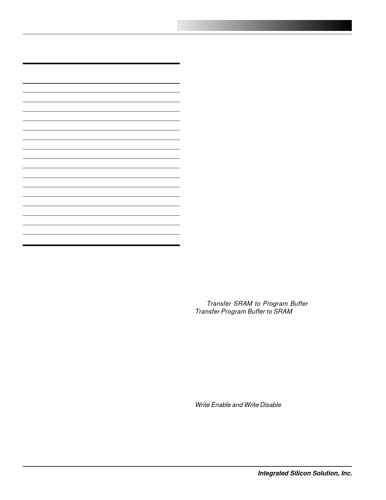
Table 2. Write Protect Range Sector Selection (Hex)
Write Protect
Range Config. Bits
WR3 WR2 WR1 WR0
00 00
00 01
00 10
00 11
01 00
01 01
01 10
01 11
10 00
10 01
10 10
10 11
11 00
11 01
11 10
11 11
Write Protected Sectors
WD=0
WD=1
None
None
000 - 01FH x E0 - 1FF/ 3FF/ 7FFH
000 - 03FH x C0 - 1FF/ 3FF/ 7FFH
000 - 05FH x A0 - 1FF/ 3FF/ 7FFH
000 - 07FH x 80 - 1FF/ 3FF/ 7FFH
000 - 09FH x 60 - 1FF/ 3FF/ 7FFH
000 - 0BFH x 40 - 1FF/ 3FF/ 7FFH
000 - 0DFH x 20 - 1FF/ 3FF/ 7FFH
000 - 0FFH x 00 - 1FF/ 3FF/ 7FFH
000 - 11FH y E0 - 1FF/ 3FF/ 7FFH
000 - 13FH y C0 - 1FF/ 3FF/ 7FFH
000 - 15FH y A0 - 1FF/ 3FF/ 7FFH
000 - 17FH y 80 - 1FF/ 3FF/ 7FFH
000 - 19FH y 60 - 1FF/ 3FF/ 7FFH
000 - 1BFH y 40 - 1FF/ 3FF/ 7FFH
ALL
ALL
Note:
1. IS25F041A x=7 Y=6, IS25F021A x=3 y=2,
and IS25F011A x=1 y=0
HOLD-R/B, HR[1:0]
The Hold-Ready/Busy (HOLD-R/B) bits HR1 and HR0 are
located at bits CF[1:0] of the configuration register. These
two bits select one of four possible functions: No Connect,
HOLD input, R/B Output, or R/B Output with open drain. The
factory setting for the pin is “No Connect”.
HR1 HR0 Pin Configuration
0
0
HOLD input
0
1
No Connect
1
0
R/B Output (Open Drain)
1
1
R/B Output
Configured as a R/B output, the pin can serve as a system
interrupt. When R/B is high, the array is ready to be
programmed. When R/B is low, it is busy programming.
If configured with an open-drain, an external pull-up
resistor should be used.
As a HOLD input, the pin can be used in conjunction with
the CS and SCK pin to suspend a serial command
sequence without resetting the command. This can be
useful if a command is in process and a higher priority
task on the same SPI bus needs to be attended to. To
suspend a command, HOLD must be brought low while
CS and SCK are low. With HOLD low, further data on the
SI pin is ignored (even while SCK is clocked) and the SO
pin goes to a high-impedance state. To resume the
command sequence, HOLD must be brought high when
CS and SCK are low. See timing diagrams.
Status Register Bit Descriptions
The status register provides status of the Flash array’s
Ready/Busy condition (R/B), transfers between the SRAM
and program buffer (TX), Write-Enable/Disable (WE),
and Compare Not Equal (CNE). The register can be read
using the Read Status Register command (Figure 8).
Ready/Busy Status, BUSY
The BUSY status bit is located at bit ST[7] of the status
register. Testing the BUSY bit is one of several ways to
check Ready/Busy status of the array. At power-up the
BUSY bit is reset to 0.
BUSY=1 The memory array is busy programming.
BUSY=0 The memory array is ready for further use.
SRAM and Program Buffer Transfer, TR
The TR status bit is located at bit ST[6] of the status
register. The bit provides status primarily for use during
the Transfer SRAM to Program Buffer command and
Transfer Program Buffer to SRAM command. An active
state 1 indicates a transfer is in process and the SRAM
or Program Buffer is not available for use. The device
will indicate a BUSY state while the TR bit is active.
Upon power up the TR bit resets to 0.
TR=1 SRAM and Program Buffer Transferring.
TR=0 SRAM and Program Buffer Not Transferring.
Write Enable/Disable, WE
The WE status bit is located at bit ST[4] of the status
register. The bit provides write protect status of global
Write Enable and Write Disable commands. Upon power-
up the WE bit resets to 0.
WE=1 Write Enabled, array can be written to.
WE=0 Write Disabled, array can not be written to.
8
Integrated Silicon Solution, Inc.
PRELIMINARY SF001-1A
06/24/98