IS25F011A Ver la hoja de datos (PDF) - Integrated Silicon Solution
Número de pieza
componentes Descripción
Fabricante
IS25F011A
Integrated Silicon Solution

IS25F011A Datasheet PDF : 23 Pages
| |||
IS25F011A
IS25F021A
IS25F041A
The Compare Sector command allows the contents of the
SRAM to be compared with the specified sector in memory.
The result of the compare is set in the status register. This
command can be useful when rewriting multi-sector files
that have only minor changes from the previous write. If the
new data in the SRAM is the same as the previously
written data, the sector write can be skipped. Used in this
way, the command saves time that would have been
used for re-programming. It also extends the endurance
of the Flash memory cells. The Compare Sector command
is also useful for write/verify operation (see High Data
Integrity Applications, page 19).
Using the SRAM Independant of Flash Memory
The SRAM can be used independently of Flash memory
operations for lookup tables, variable storage, or scratch
pad purposes. If the Flash memory needs to be written to
while SRAM is being used for a different purpose, the
contents can be temporarily stored to a sector and then
transferred back again when needed. The SRAM can be
especially useful for RAM-limited microcontroller-based
systems, eliminating the need for external SRAM and
freeing pins for other purposes. It can also make it possible
to use small pin-count microcontrollers, since only a few
pins are needed for the interface instead of the 20-40 pins
required for parallel bus-oriented Flash devices.
If more than 264 bytes of SRAM are needed, the Transfer
SRAM to Program Buffer, Transfer Program Buffer to
ISSI ®
SRAM, and the Read Program Buffer commands can be
used to expand the storage to 528 bytes. In this mode of
operation, all writes must be handled through the 264-byte
SRAM and the Program buffer is essentially used as a
stack.
Write Protection
The IS25F011A, IS25F021A, and IS25F041A provide
advanced software and hardware write protection fea-
tures. Software-controlled write protection of the entire
array is handled using the Write Enable and Write Disable
commands. Hardware write protection is possible using
the Write Protect pin (WP). Write-protecting a portion of
Flash memory is accommodated by programming a write
protect range in the configuration register. For applica-
tions needing a portion of the memory to be permanently
write-protected, a onetime programmable write protec-
tion feature is supported. Contact ISSI for further informa-
tion.
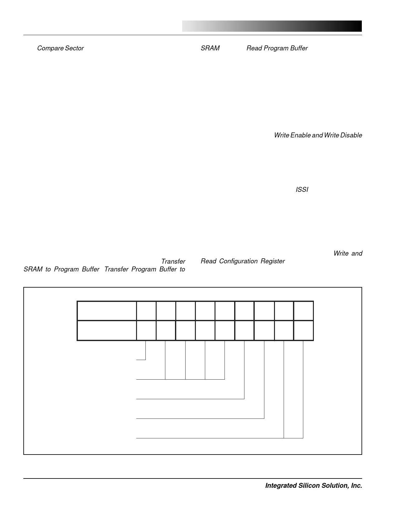
Configuration Register
The Configuration Register stores the current configura-
tion of the HOLD-R/B pin, read clock edge, write protect
range, and alternate oscillator frequency (Figure 6). The
configuration register is accessed using the Write and
Read Configuration Register commands. A nonvolatile
CF15:9
(RESERVED)
CF8 CF7 CF6 CF5 CF4 CF3 CF2 CF1 CF0
AF WR3 WR2 WR1 WR0 WD RCE HR1 HR0
ALTERNATE OSCILATOR
FREQUENCY
WRITE PROTECT
RANGE
WRITE PROTECT
DIRECTION
READ DATA
CLOCK EDGE
HOLD-READY/BUSY
PIN FUNCTION
Figure 6. Configuration Register Bit Locations
6
Integrated Silicon Solution, Inc.
PRELIMINARY SF001-1A
06/24/98
Share Link: