IS25F011A Ver la hoja de datos (PDF) - Integrated Silicon Solution
Número de pieza
componentes Descripción
Fabricante
IS25F011A
Integrated Silicon Solution

IS25F011A Datasheet PDF : 23 Pages
| |||
IS25F011A
IS25F021A
IS25F041A
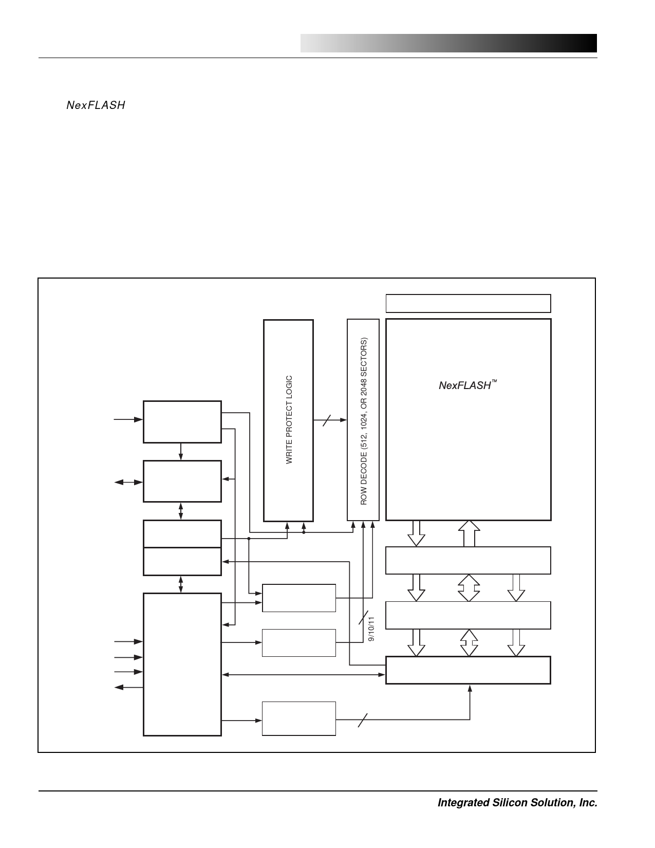
FUNCTIONAL OVERVIEW
The NexFLASH TM IS25F011A, IS25F021A, and
IS25F041A Serial Flash memories provide up to 1M-bit,
2M-bit, and 4M-bit respectively, of low-power and low-
voltage nonvolatile memory that is fully accessible through
a 4-pin Serial Peripheral Interface (SPI) bus. The
IS25F011A, IS25F021A, and IS25F041A incorporate a
variety of special features, such as on-board Serial SRAM,
advanced write protection, and electronic device identifi-
cation.
ISSI ®
An architectural block diagram of the IS25F011A,
IS25F021A, and IS25F041A is shown in Figure 2. Key
elements of the architecture include:
• SPI Interface and Command Set Logic
• Serial Flash Memory Array
• Serial SRAM and Program Buffer
• Write Protection Logic
• Configuration and Status Registers
DEVICE INFORMATION SECTOR
WP
HOLD
OR R/B
WRITE CONTROL
LOGIC
HOLD OR
READ/BUSY
LOGIC
1, 2, or 4 MEGABIT
SERIAL FLASH MEMORY ARRAY
16
512, 1024, OR 2048 BYTE-ADDRESSABLE
SECTORS OF 264 BYTES EACH
CONFIGURATION
REGISTER
STATUS
REGISTER
SCK
CS
SI
SO
SPI
COMMAND
AND
CONTROL
LOGIC
HIGH-VOLTAGE
GENERATORS
SECTOR-ADDRESS
LATCH
DATA
BYTE-ADDRESS
LATCH/COUNTER
2112
PROGRAM BUFFER
(264 BYTES)
2112
SRAM
(264 BYTES)
8
8
8
COLUMN DECODE, SENSE AMP LATCH
AND DATA COMPARE LOGIC
9
Figure 2. IS25F011A, IS25F021A, and IS25F041A Architectural Block Diagram
2
Integrated Silicon Solution, Inc.
PRELIMINARY SF001-1A
06/24/98
Share Link: