IS25F011A Ver la hoja de datos (PDF) - Integrated Silicon Solution
Número de pieza
componentes Descripción
Fabricante
IS25F011A
Integrated Silicon Solution

IS25F011A Datasheet PDF : 23 Pages
| |||
IS25F011A
IS25F021A
IS25F041A
ISSI ®
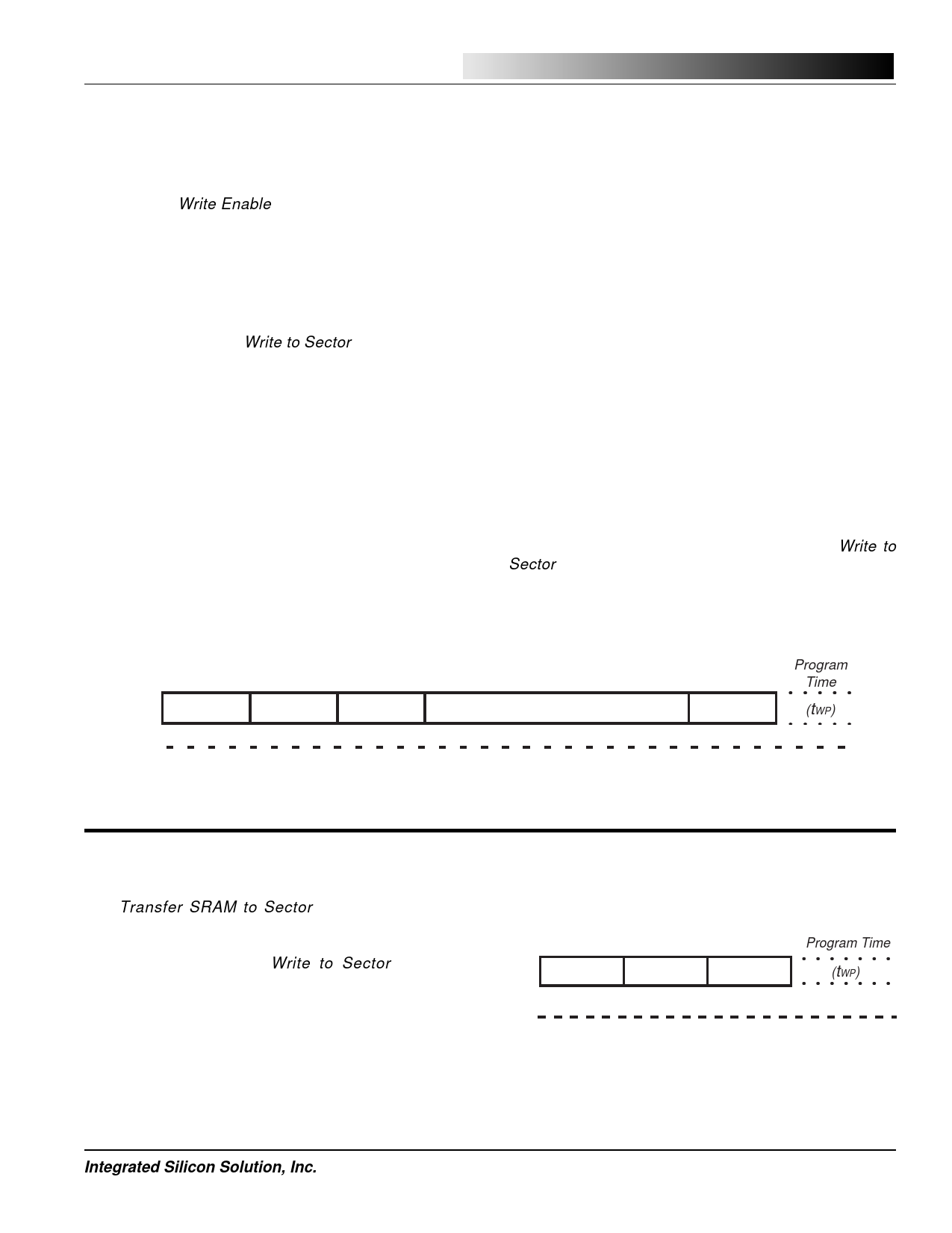
Write to Sector
Before writing to a sector in the Flash memory array, all
hardware and software write protection must be in an
enabled state. This means that the WP pin must be in a
high state, a Write Enable command must have previ-
ously been issued, and the sector location that is to be
written to must be outside the write protect range set in
the configuration register. Additionally, the Ready/Busy
status should be checked to confirm that the memory
array is available to be written to.
The bit order within each byte is most significant bit first
1 (i.e., D7,...D0). The byte-address is automatically in-
cremented to the next higher byte address as the clock
continues. When the last byte address to be written is
reached, the command can be completed with an
additional eightcontrol clocks (with data=0) followed by
2 asserting CS high. If the clock continues to increment
past the highest byte-address (107H), the address
counter will roll over to byte 0H.
Writing to a sector is accomplished by first bringing CS
low and shifting in the Write to Sector command (F3H)
followed by a 16-bit “sector-address” field. Although the
sector-address field is 16-bits, only bits S[8:0] for the
IS25F011A (0-1FFH), S[9:0] for the IS25F021A (0-3FFH),
or S[10:0] for the IS25F041A (0-7FFH) are used. The
uppermost sector address bits are not used but must be
clocked in (use 0 data). Following the sector address, a
16-bit “byte-address” field is clocked into the device to
designate the starting location within the 264-byte sector.
Only bits B[8:0] of the byte-address field are used and
only values of 0-107H (264 bytes) are valid.
After the byte-address has been loaded, data is shifted
into the 264-byte SRAM, which serves as a temporary
storage buffer. Existing data in the SRAM will be written
over. The byte order of the data shifted into the SRAM
is least significant byte first (i.e., byte-00H, byte-01H,...).
3 After the CS pin is brought high, the data in the SRAM
is automatically transferred to the Program Buffer, which
handles the self-timed programming of the specified
sector in memory array. See tWP timing specifications.
4 During this time the array will be “busy” and will ignore
further array-related commands until complete. All
Ready/Busy status indicators will indicate a busy sta-
tus. Since the Program Buffer handles all array pro-
gramming, the SRAM is still available to be read from or
5 written to during the busy state. Applications that require
high data integrity should verify written sectors or use other
techniques such as ECC (see High Data Integrity Applica-
tions, page 19). Detailed clock timing for the Write to
Sector command is shown in Figure 11.
6
Write to
Sector
Command
Sector
Address*
Byte
Address**
Write Sector Data
Program
7
8 Clocks
Time
SI
F3H
SO
S[15:0]
B[15:0]
First Byte - Last Byte
00H
(tWP)
8
*The sector address only uses bits [8:0], [9:0] or [10:0]
**The byte address only uses bits [8:0]
9
Transfer SRAM to Sector
The Transfer SRAM to Sector command (F3H) will
write the existing contents of the SRAM to the speci-
fied sector in memory. The command sequence is
identical to that of the Write to Sector command
except that immediately after the sector address field
S[15:0] and 16 control clocks, the CS pin is asserted
high. This automatically transfers the 264-bytes of
SRAM data to the Program Buffer, which handles the
programming of the specified sector in the memory
array. During this time, the array will be busy. Since the
entire 264-bytes are transferred, the byte-address field
B[15:0] is not used.
Transfer SRAM
to Sector
Sector
Command Address*
SI
F3H
S[15:0]
16 Clocks
0000H
10
Program Time
(tWP)
11
SO
12
*The sector address only uses bits [8:0] or [10:0]
Integrated Silicon Solution, Inc.
13
PRELIMINARY SF001-1A
06/24/98
Share Link: