IRF630NLTRLPBF Ver la hoja de datos (PDF) - International Rectifier
N√∫mero de pieza
componentes Descripción
Fabricante
IRF630NLTRLPBF Datasheet PDF : 11 Pages
| |||
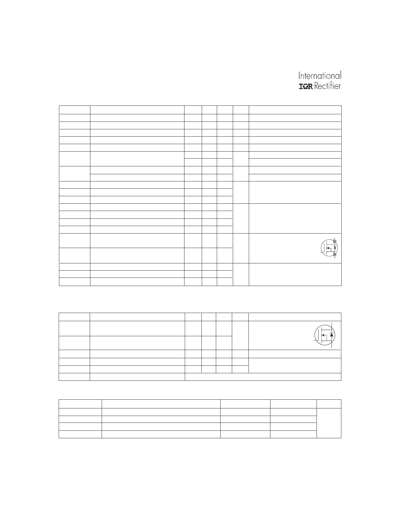
IRF630N/S/LPbF
Electrical Characteristics @ TJ = 25°C (unless otherwise specified)
V(BR)DSS
∆V(BR)DSS/∆TJ
RDS(on)
VGS(th)
gfs
Parameter
Drain-to-Source Breakdown Voltage
Breakdown Voltage Temp. Coefficient
Static Drain-to-Source On-Resistance
Gate Threshold Voltage
Forward Transconductance
IDSS
Drain-to-Source Leakage Current
IGSS
Qg
Qgs
Qgd
td(on)
tr
td(off)
tf
Gate-to-Source Forward Leakage
Gate-to-Source Reverse Leakage
Total Gate Charge
Gate-to-Source Charge
Gate-to-Drain ("Miller") Charge
Turn-On Delay Time
Rise Time
Turn-Off Delay Time
Fall Time
LD
Internal Drain Inductance
LS
Ciss
Coss
Crss
Internal Source Inductance
Input Capacitance
Output Capacitance
Reverse Transfer Capacitance
Min.
200
–––
–––
2.0
4.9
–––
–––
–––
–––
–––
–––
–––
–––
–––
–––
–––
–––
–––
–––
–––
–––
Typ.
–––
0.26
–––
–––
–––
–––
–––
–––
–––
–––
–––
–––
7.9
14
27
15
4.5
7.5
575
89
25
Max.
–––
–––
0.30
4.0
–––
25
250
100
-100
35
6.5
17
–––
–––
–––
–––
–––
–––
–––
–––
–––
Units
V
V/°C
Ω
V
S
µA
nA
nC
ns
nH
pF
Conditions
VGS = 0V, ID = 250µA
Reference to 25°C, ID = 1mA
VGS = 10V, ID = 5.4A ƒ
VDS = VGS, ID = 250µA
VDS = 50V, ID = 5.4A ƒ
VDS = 200V, VGS = 0V
VDS = 160V, VGS = 0V, TJ = 150°C
VGS = 20V
VGS = -20V
ID = 5.4A
VDS = 160V
VGS = 10V ƒ
VDD = 100V
ID = 5.4A
RG = 13Ω
RD = 18Ω ƒ
Between lead,
D
6mm (0.25in.)
from package
G
and center of die contact
S
VGS = 0V
VDS = 25V
ƒ = 1.0MHz
Source-Drain Ratings and Characteristics
Parameter
IS
Continuous Source Current
(Body Diode)
ISM
Pulsed Source Current
(Body Diode)
VSD
Diode Forward Voltage
trr
Reverse Recovery Time
Qrr
Reverse Recovery Charge
ton
Forward Turn-On Time
Min. Typ. Max. Units
Conditions
MOSFET symbol
D
––– ––– 9.3
A showing the
integral reverse
G
––– ––– 37
p-n junction diode.
S
––– ––– 1.3 V TJ = 25°C, IS = 5.4A, VGS = 0V ƒ
––– 117 176 ns TJ = 25°C, IF = 5.4A
––– 542 813 nC di/dt = 100A/µs ƒ
Intrinsic turn-on time is negligible (turn-on is dominated by LS+LD)
Thermal Resistance
RθJC
RθCS
RθJA
RθJA
Parameter
Junction-to-Case
Case-to-Sink, Flat, Greased Surface „
Junction-to-Ambient„
Junction-to-Ambient (PCB mount)¬Ö
Typ.
–––
0.50
–––
–––
Max.
1.83
–––
62
40
Units
°C/W
www.irf.com
2
Share Link: 