X2804CP-15 Ver la hoja de datos (PDF) - Xicor -> Intersil
Número de pieza
componentes Descripción
Fabricante
X2804CP-15 Datasheet PDF : 13 Pages
| |||
X2804C
PIN DESCRIPTIONS
Addresses (A0–A8)
The Address inputs select an 8-bit memory location
during a read or write operation.
Chip Enable (CE)
The Chip Enable input must be LOW to enable all
read/write operations. When CE is HIGH, power con-
sumption is reduced.
Output Enable (OE)
The Output Enable input controls the data output buffers
and is used to initiate read operations.
PIN NAMES
Symbol
A0–A8
I/O0–I/O7
WE
CE
OE
VCC
VSS
NC
Description
Address Inputs
Data Input/Output
Write Enable
Chip Enable
Output Enable
+5V
Ground
No Connect
6612 PGM T01
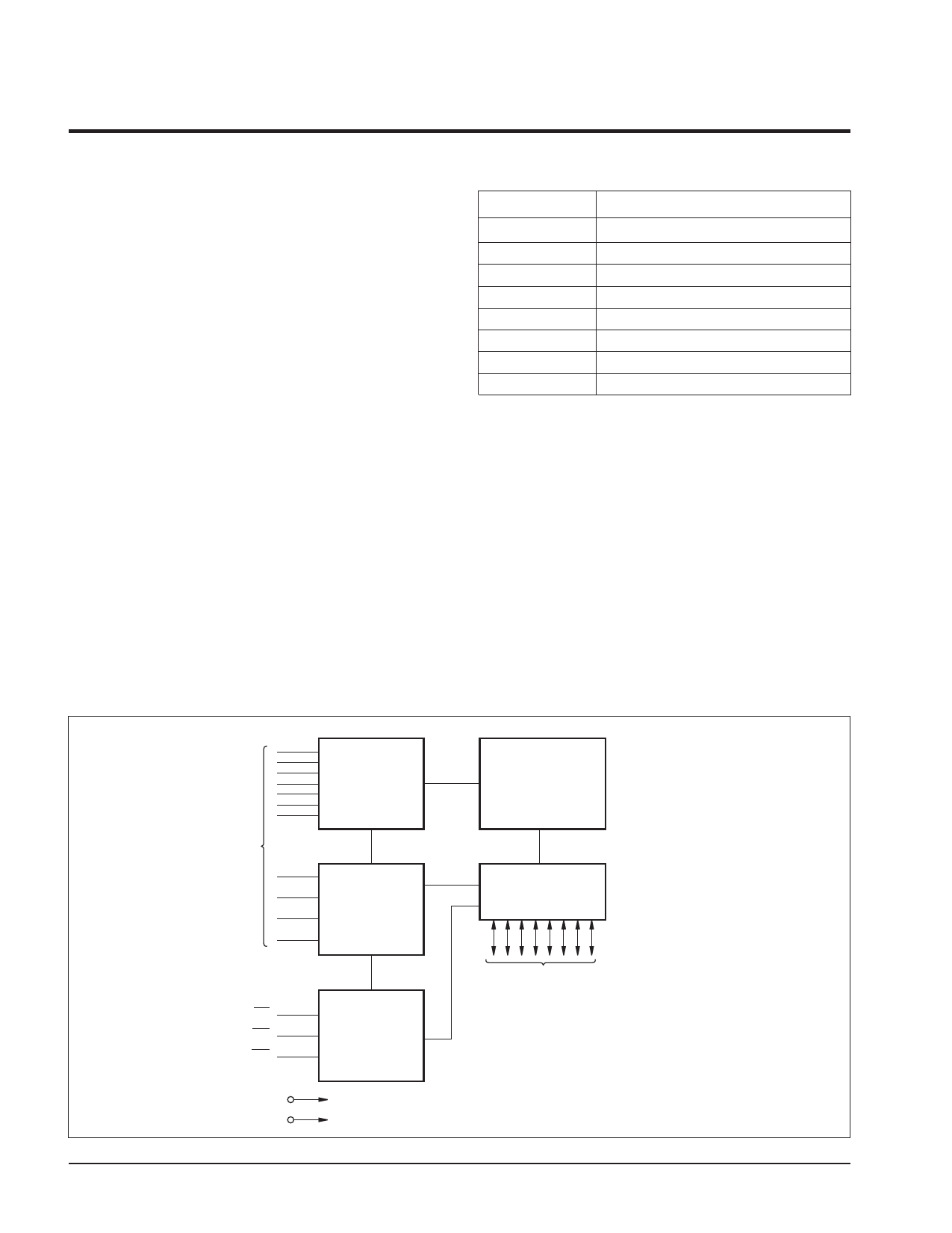
FUNCTIONAL DIAGRAM
A0–A8
ADDRESS
INPUTS
X BUFFERS
LATCHES AND
DECODER
Y BUFFERS
LATCHES AND
DECODER
CE
OE
WE
VCC
VSS
CONTROL
LOGIC
4.096-BIT
E2PROM
ARRAY
I/O BUFFERS
AND LATCHES
I/O0–I/O7
DATA INPUTS/OUTPUTS
6612 FHD F01
2
Share Link: 