ST93CS66 Ver la hoja de datos (PDF) - STMicroelectronics
Número de pieza
componentes Descripción
Fabricante
ST93CS66 Datasheet PDF : 16 Pages
| |||
ST93CS66, ST93CS67
POWER-ON DATA PROTECTION
In order to prevent data corruption and inadvertent
write operations during power up, a Power On
Reset (POR) circuit resets all internal programming
circuitry and sets the device in the Write Disable
mode. When VCC reaches its functional value, the
device is properlyreset (in the Write Disable mode)
and is ready to decode and execute an incoming
instruction. A stable VCC must be applied before
any logic signal.
INSTRUCTIONS
The ST93CS66/67 has eleven instructions, as
shown in Table 6. Each instruction is composed of
a 2 bit op-code and an 8 bit address. Each instruc-
tion is preceded by the rising edge of the signal
applied on the Chip Select (S) input (assuming that
the Clock C is low). The data input D is then
sampled upon the following rising edges of the
clock C until a ’1’ is sampled and decoded by the
ST93CS66/67 as a Start bit.
The ST93CS66/67 is fabricated in CMOS technol-
ogy and is therefore able to run from zero Hz (static
input signals) up to the maximum ratings (specified
in Table 5).
Read
The Read instruction (READ) outputs serial data
on the Data Output (Q). When a READ instruction
is received, the instruction and address are de-
coded and the data from the memory is transferred
into an output shiftregister. A dummy ’0’ bit is output
first followed by the 16 bit word with the MSB first.
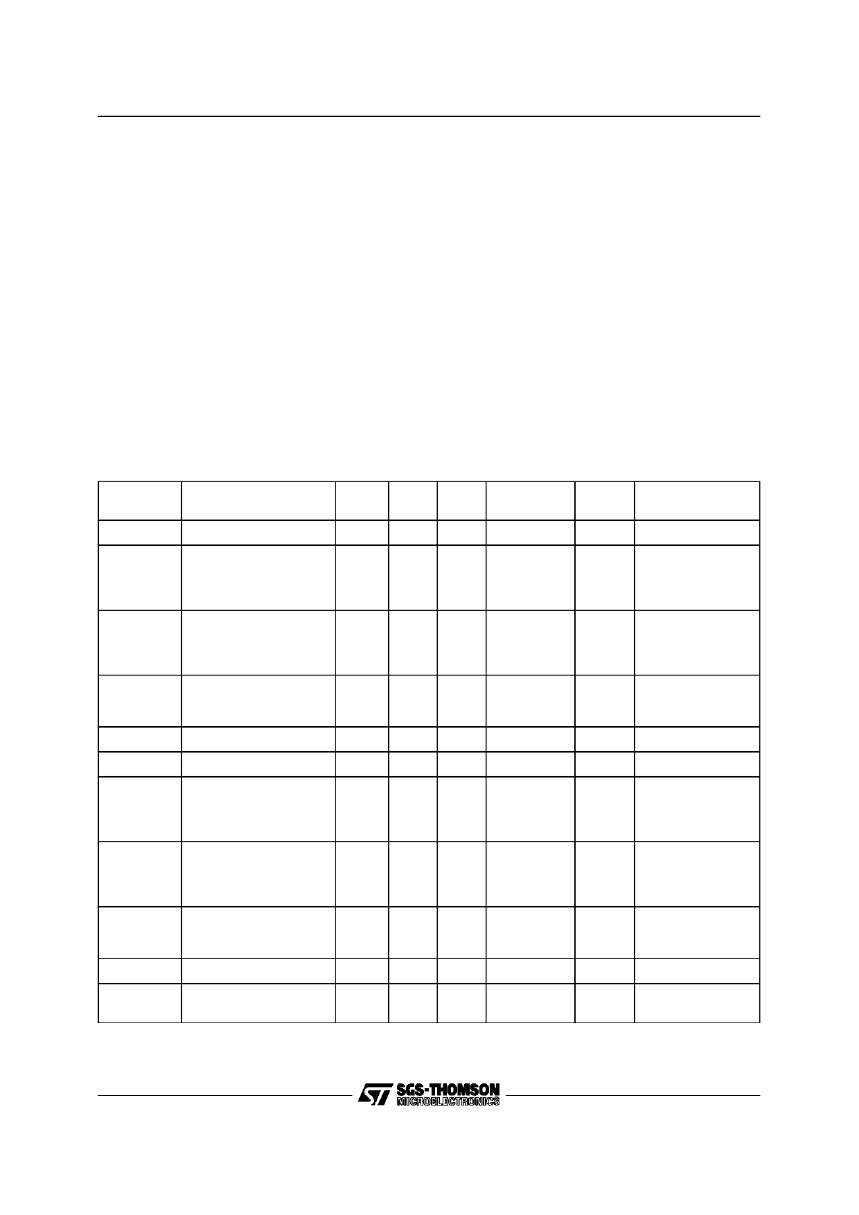
Table 6. Instruction Set
Instruction
Description
READ Read Data from Memory
WRITE Write Data to Memory
PAWRITE Page Write to Memory
WRALL Write All Memory
WEN
WDS
Write Enable
Write Disable
PRREAD Protect Register Read
PRWRITE Protect Register Write
PRCLEAR Protect Register Clear
PREN Protect Register Enable
PRDS Protect Register Disable
Note: 1. X = don’t care bit.
W
pin (1)
X
’1’
’1’
’1’
’1’
X
X
’1’
’1’
’1’
’1’
PRE
pin
’0’
’0’
’0’
’0’
’0’
’0’
’1’
’1’
’1’
’1’
’1’
Op
Code
10
01
11
00
00
00
10
01
11
00
00
Address (1)
A7-A0
A7-A0
A7-A0
01XX XXXX
11XX XXXX
00XX XXXX
XXXX XXXX
A7-A0
1111 1111
11XX XXXX
0000 0000
Data
Additional
Information
Q15-Q0
D15-D0
Write is executed if
the address is not
inside the
Protected area
D15-D0
Write is executed if
all the addresses
are not inside the
Protected area
Write all data if the
D15-D0 Protect Register is
cleared
Q8-Q0
Data Output =
Protect Register
content + Protect
Flag bit
Data above
specified address
A7-A0 are
protected
Protect Flag is also
cleared (cleared
Flag = 1)
OTP bit is set
permanently
6/16
Share Link: 