ILC7080 Ver la hoja de datos (PDF) - Impala Linear Corporation
Número de pieza
componentes Descripción
Fabricante
ILC7080 Datasheet PDF : 16 Pages
| |||
50/100mA SOT-23 CMOS RF LDO™ Regulators
The Effects of ESR (Equivalent Series Resistance)
The ESR of a capacitor is a measure of the resistance due
to the leads and the internal connections of the component.
Typically measured in mΩ (milli-ohms) it can increase to
ohms in some cases.
Wherever there is a combination of resistance and current,
voltages will be present. The control functions of LDOs use
two voltages in order to maintain the output precisely; VOUT
and VREF.
With reference to the block diagram in figure 2, VOUT is fed
back to the error amplifier and is used as the supply volt-
age for the internal components of the 7080/81. So any
change in VOUT will cause the error amplifier to try to com-
pensate to maintain VOUT at the set level and noise on
VOUT will be reflected into the supply of each internal cir-
cuit. The reference voltage, VREF, is influenced by the
CNOISE pin. Noise into this pin will add to the reference volt-
age and be fed through the circuit. These factors will not
cause a problem if some simple steps are taken. Figure 5
shows where these added ESR resistances are present in
the typical LDO circuit.
VOUT
IOUT
IC RC 5 SOT23-5 4
R*
COUT
ILC7080
ILC7081
CNOISE
VIN
1
2
3
R*
CIN
RF LDOTM ON
Regulator
OFF
Figure 5: ESR in COUT and CNOISE
With this in mind low ESR components will offer better per-
formance as LDOs may be exposed to large transients of
output voltage, and current flows through the capacitors in
order to filter these transient swings. ESR is less of a prob-
lem with CIN as the voltage fluctuations at the input will be
filtered by the LDO.
However, being aware of these current flows, there is also
another potential source of induced voltage noise from the
resistance inherent in the PCB trace. Figure 6 shows where
the additive resistance of the PCB can manifest itself. Again
these resistances may be very small, but a summation of
several currents can develop detectable voltage ripple and
will be amplified by the LDO. Particularly the accumulation
of current flows in the ground plane can develop significant
voltages unless care is taken.
With a degree of care, the ILC7080/81 will yield outstanding
performance.
Printed Circuit Board Layout Guidelines
As was mentioned in the previous section, to take full
advantage of any high performance LDO regulator requires
paying careful attention to grounding and printed circuit
board (PCB) layout.
VOUT IOUT
RPCB
I1
COUT
I2
RPCB
RPCB
5 SOT23-5 4
ILC7080
ILC7081
ESR
CNOISE
VIN
1
VIN
RPCB
2
3
RPCB ON
OFF
Figure 6: Inherent PCB resistance
Figure 7 shows the effects of poor grounding and PCB lay-
out caused by the ESR and PCB resistances and the accu-
mulation of current flows.
Note particularly that during high output load current, the
LDO regulator’s ground pin and the ground return for COUT
and CNOISE are not at the same potential as the system
ground. This is due to high frequency impedance caused by
PCB’s trace inductance and DC resistance. The current
loop between COUT, CNOISE and the LDO regulator’s ground
pin will degrade performance of the LDO.
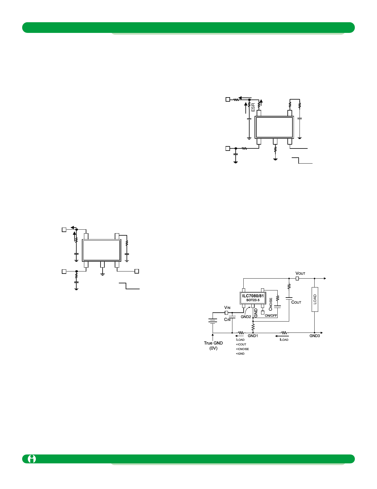
5
4
12 3
Figure 7: Effects of poor circuit layout
Figure 8 shows an optimum schematic. In this schematic,
high output surge current has little effect on the ground cur-
rent and noise bypass current return of the LDO regulator.
Note that the key difference here is that COUT and CNOISE
are directly connected to the LDO regulator’s ground pin.
The LDO is then separately connected to the main ground
plane and returned to a single point system ground.
The layout of the LDO and its external components are also
based on some simple rules to minimize EMI and output
voltage ripple.
Impala Linear Corporation
ILC7080/81 1.1
(408) 574-3939 www.impalalinear.com
Sept. 1998 8
Share Link: 