IL34119 Ver la hoja de datos (PDF) - Integral Corp.
Número de pieza
componentes Descripción
Fabricante
IL34119 Datasheet PDF : 6 Pages
| |||
IL34119
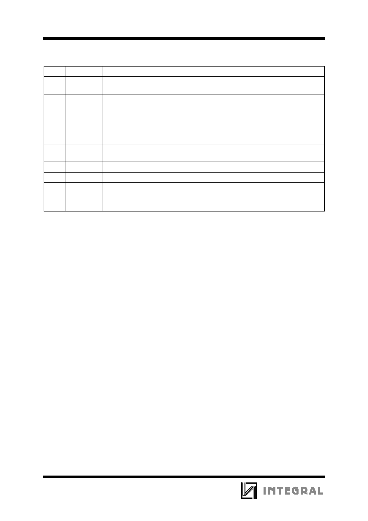
PIN DESCRIPTION
Pin Symbol
Description
1
CD
Chip Disable - Digital input. A Logic “0” (<0.8 V) sets normal operation. A Logic “1”
(≥2.0 V) sets the power down mode. Input impedance is nominally 90 KΩ.
2
FC2
A capacitor at this pin increases power supply rejection, and affects turn-on time. This
pin can be left open if the capacitor at FC1 is sufficient.
3
FC1
Analog Ground for the amplifiers. A 1.0 µF capacitor at this pin (with a 5.0 µF
capacitor at Pin 2) provides 52 dB of power supply rejection. Turn-on time of the
circuit is affected by the capacitor on this pin. This pin can be used as an alternate
input.
4
VIN
Amplifier input. The input capacitor and resistor set low frequency rolloff and input
impedance. The feedback resistor is connected to this pin and VO1.
5
VO1
Amplifier Output #1. The dc level is ≈ (VCC - 0.7 V)/2.
6
VCC
DC supply voltage (+2.0 to +16 Volts) is applied to this pin.
7
GND Ground pin for the entire circuit.
8
VO2
Amplifier Output #2. This signal is equal in amplitude, but 180° out of phase with that
at VO1. The dc level is ≈ (VCC - 0.7 V)/2.
DESIGN GUIDELINES
GENERAL
The IL34119 is a low power audio amplifier
capable of low voltage operation (VCC = 2.0 V
minimum) such as that encountered in line-powered
speakerphones. The circuit provides a differential
output (VO1-VO2) to the speaker to maximize the
available voltage swing at low voltages. The
differential gain is set by two external resistors. Pins
FC1 and FC2 allow controlling the amount of power
supply and noise rejection, as well as providing
alternate inputs to the amplifiers. The CD pin permits
powering down the IC for muting purposes and to
conserve power.
AMPLIFIERS
Referring to the block diagram, the internal
configuration consists of two identical operational
amplifiers. Amplifier #1 has an open-loop gain of
≥80 dB (at f ≤ 100 Hz), and the closed loop gain is
set by external resistors Rf and Ri. The amplifier is
unity gain stable, and has a unity gain frequency of
approximately 1.5 MHz. In order to adequately cover
the telephone voice band (300-340 Hz), a maximum
closed loop gain of 46 dB is recommended. Amplifier
#2 is internally set to a gain of -1.0 (0 dB).
The outputs of both amplifiers are capable of
sourcing and sinking a peak current of 200 mA. The
outputs can typically swing to within ≈0.4 volts above
ground, and to within ≈1.3 volts below VCC, at the
maximum current. The output dc offset voltage
(VO1-VO2) is primarily a function of the feedback
resistor (Rf), and secondarily due to the amplifiers’
input offset voltages. The input offset voltage of the
two amplifiers will generally be similar for a
particular IC, and therefore nearly cancel each other
at the outputs. Amplifier #1’s bias current, however,
flows out of VIN (Pin 4) and through Rf, forcing VO1
to shift negative by an amount equal to [Rf x IIB].
VO2 is shifted positive an equal amount. The output
offset voltage specified in the Electrical
Characteristics is measured with the feedback resistor
shown in the Simplified Block Diagram, and
therefore takes into account the bias current as well as
internal offset voltages of the amplifiers. The bias
current is constant with respect to VCC.
FC1 and FC2
Power supply rejection is provided by the
capacitors (C1 and C2 in the Simplified Block
Diagram) at FC1 and FC2. C2 is somewhat dominant
at low frequencies, while C1 is dominant at high
frequencies. The reguired values of C1 and C2
depend on the conditions of each application. A
2
Share Link: 