IDTQS3126 Ver la hoja de datos (PDF) - Integrated Device Technology
NÚmero de pieza
componentes DescripciÃģn
Fabricante
IDTQS3126
Integrated Device Technology

IDTQS3126 Datasheet PDF : 5 Pages
| |||
IDTQS3126
HIGH-SPEED CMOS QUADRUPLE BUS SWITCH WITH INDIVIDUAL ACTIVE
INDUSTRIAL TEMPERATURE RANGE
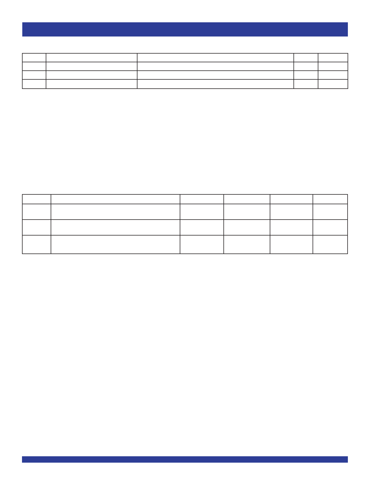
POWER SUPPLY CHARACTERISTICS
Symbol
Parameter
Test Conditions(1)
Max.
Unit
ICCQ Quiescent Power Supply Current
VCC = Max., VIN = GND or VCC, f = 0
âICC Power Supply Current per Input HIGH(2)
VCC = Max., VIN = 3.4V, f = 0
ICCD Dynamic Power Supply Current per MHz (3) VCC = Max., A and Y Pins Open, Control Inputs Toggling @ 50% Duty Cycle
3
ÂĩA
1.25
mA
0.25 mA/MHz
NOTES:
1. For conditions shown as Min. or Max., use the appropriate values specified under DC Electrical Characteristics.
2. Per TTL-driven input (VIN = 3.4V, control inputs only). A and Y pins do not contribute to âIcc.
3. This current applies to the control inputs only and represents the current required to switch internal capacitance at the specified frequency. The A and Y inputs generate no significant
AC or DC currents as they transition. This parameter is guaranteed but not production tested.
SWITCHING CHARACTERISTICS OVER OPERATING RANGE
TA = -40°C to +85°C, VCC = 5V ¹ 5%
CLOAD = 50pF, RLOAD = 500âĶ unless otherwise noted.
Symbol
Parameter
Min. (1)
Typ.
Max.
Unit
tPLH
Data Propagation Delay(2)
tPHL
A to Y
ïĢ§
ïĢ§
0.25(3)
ns
tPZL
Switch Turn-On Delay
tPZH
OE to xA/xY
tPLZ
Switch Turn-Off Delay(2)
tPHZ
OE to xA/xY
1.5
ïĢ§
1.5
ïĢ§
6.5
ns
5.5
ns
NOTES:
1. Minimums are guaranteed but not production tested.
2. This parameter is guaranteed but not production tested.
3. The bus switch contributes no propagation delay other than the RC delay of the ON resistance of the switch and the load capacitance. The time constant for the switch alone
is of the order of 0.25ns at CL = 50pF. Since this time constant is much smaller than the rise and fall times of typical driving signals, it adds very little propagation delay to the
system. Propagation delay of the bus switch, when used in a system, is determined by the driving circuit on the driving side of the switch and its interaction with the load on
the driven side.
4
Share Link: