IDT7164L15D Ver la hoja de datos (PDF) - Integrated Device Technology
Número de pieza
componentes Descripción
Fabricante
IDT7164L15D Datasheet PDF : 9 Pages
| |||
IDT7164S/L
CMOS STATIC RAM 64K (8K x 8-BIT)
MILITARY AND COMMERCIAL TEMPERATURE RANGES
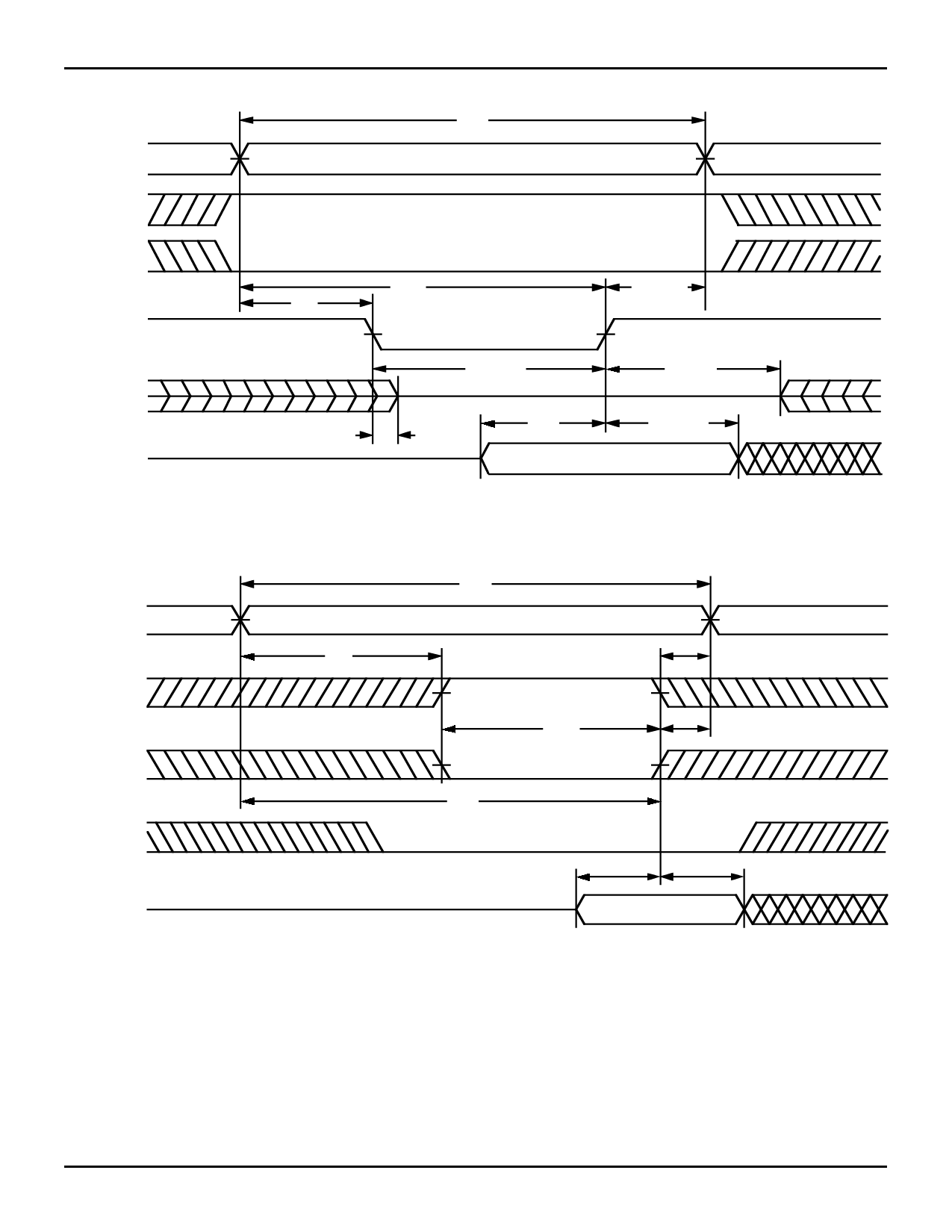
TIMING WAVEFORM OF WRITE CYCLE NO. 1 (WE CONTROLLED TIMING)(1, 2, 6)
tWC
ADDRESS
CS2
CS1
WE
DATA OUT
DATA IN
tAW
tAS
tWR1(3)
(4)
tWHZ(7)
(6)
tWP
tOW(7)
tDW
tDH1, 2
DATA VALID
2967 drw 08
TIMING WAVEFORM OF WRITE CYCLE NO. 2 (CS CONTROLLED TIMING)(1, 2)
tWC
ADDRESS
tAS
tWR2 (3)
CS2
CS1
tCW
(5)
tWR1 (3)
tAW
WE
tDW
tDH1,2
DATA IN
DATA VALID
2967 drw 09
NOTES:
1. WE, CS1 or CS2 must be inactive during all address transitions.
2. A write occurs during the overlap of a LOW WE, a LOW CS1 and a HIGH CS2.
3. tWR1, 2 is measured from the earlier of CS1 or WE going HIGH or CS2 going LOW to the end of the write cycle.
4. During this period, I/O pins are in the output state so that the input signals must not be applied.
5. If the CS1 LOW transition or CS2 HIGH transition occurs simultaneously with or after the WE LOW transition, the outputs remain in a high-impedance state.
6. OE is continuously HIGH. If OE is LOW during a WE controlled write cycle, the write pulse width must be the larger of tWP or (tWHZ +tDW) to allow the
I/O drivers to turn off and data to be placed on the bus for the required tDW. If OE is HIGH during a WE controlled write cycle, this requirement does not
apply and the minimum write pulse width is as short as the specified tWP.
7. Transition is measured ±200mV from steady state.
6.1
8
Share Link: 