IDT5V9882T Ver la hoja de datos (PDF) - Integrated Device Technology
Número de pieza
componentes Descripción
Fabricante
IDT5V9882T Datasheet PDF : 31 Pages
| |||
IDT5V9882T
3.3V EEPROM PROGRAMMABLE CLOCK GENERATOR
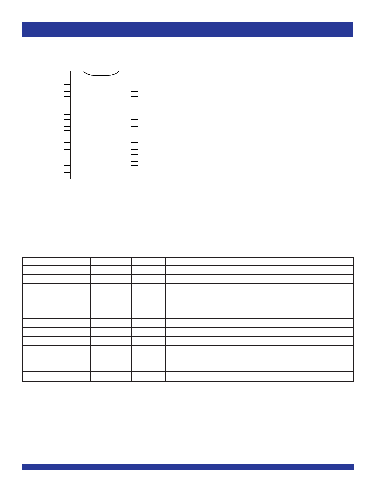
PIN CONFIGURATION
OUT2 1
VDD
2
XTALIN/REFIN 3
XTALOUT 4
OUT1 5
GND 6
OUT3 7
OUT3 8
SHUTDOWN/OE/
16 SUSPEND
15
VDD
14
I 2C_MFC
13 GIN1/SCLK
12 GIN0/SDAT
11 GND
10 OUT4
9
VDD
TSSOP
TOP VIEW
INDUSTRIAL TEMPERATURE RANGE
PIN DESCRIPTION
Pin Name
Pin# I/O
XTALIN/REFIN
3
I
XTALOUT
4
O
GIN0/SDAT
16
I
GIN1/SCLK
17
I
SHUTDOWN/OE/SUSPEND 20
I
I2C_MFC
18
I
OUT1
5
O
OUT2
1
O
OUT3
7
O
OUT3
8
O
OUT4
13
O
VDD
2, 13, 19
GND
6, 15
Type
LVTTL
LVTTL
LVTTL
LVTTL
LVTTL
3-level(1)
LVTTL
LVTTL
Adjustable(2)
Adjustable(2)
LVTTL
Description
CRYSTAL_IN - Reference crystal input or external reference clock input
CRYSTAL_OUT -Reference crystal feedback
Multi-purpose inputs. Can be used for Frequency Control or SDAT(I2C).
Multi-Purpose inputs. Can be used for Frequency Control or SDAT(I2C).
Enables/disables the outputs, PLLs or powers down the chip.
I2C (HIGH) or MFC Mode (MID)
Configurable clock output 1. Can also be used to buffer the reference clock.
Configurable clock output 2
Configurable clock output 3, Single-Ended or Differential when combined with OUT3
Configurable complementary clock output 3, Single-Ended or Differential when combined with OUT3
Configurable clock output 4
3.3V Power Supply
Ground
NOTES:
1. 3-level inputs are static inputs and must be tied to VDD or GND or left floating. These inputs are internally biased to VDD/2. They are not hot-insertable or over voltage tolerant.
2. Outputs are user programmable to drive single-ended 3.3V LVTTL, differential LVDS, or differential LVPECL interface levels.
3
Share Link: 