HWD075DGE-A(2003) Ver la hoja de datos (PDF) - Power-One Inc.
Número de pieza
componentes Descripción
Fabricante
HWD075DGE-A Datasheet PDF : 12 Pages
| |||
HWD DC/DC Series Data Sheet
HWD15DGE Power Dissipation vs Full Load Power Distribution
20
18
16
14
Po
we
r 12
Di
ss
ip 10
ati
on
(W 8
)
6
4
2
0
15/0.5
7.5/7.5
Output Load, Io1/Io2 (A)
0.5/15
Figure 6. Power Dissipation Vs. Full-Load Distribution
Characteristic Curves
Tb = 40 ºC, nominal input voltage, and rated load unless otherwise specified.
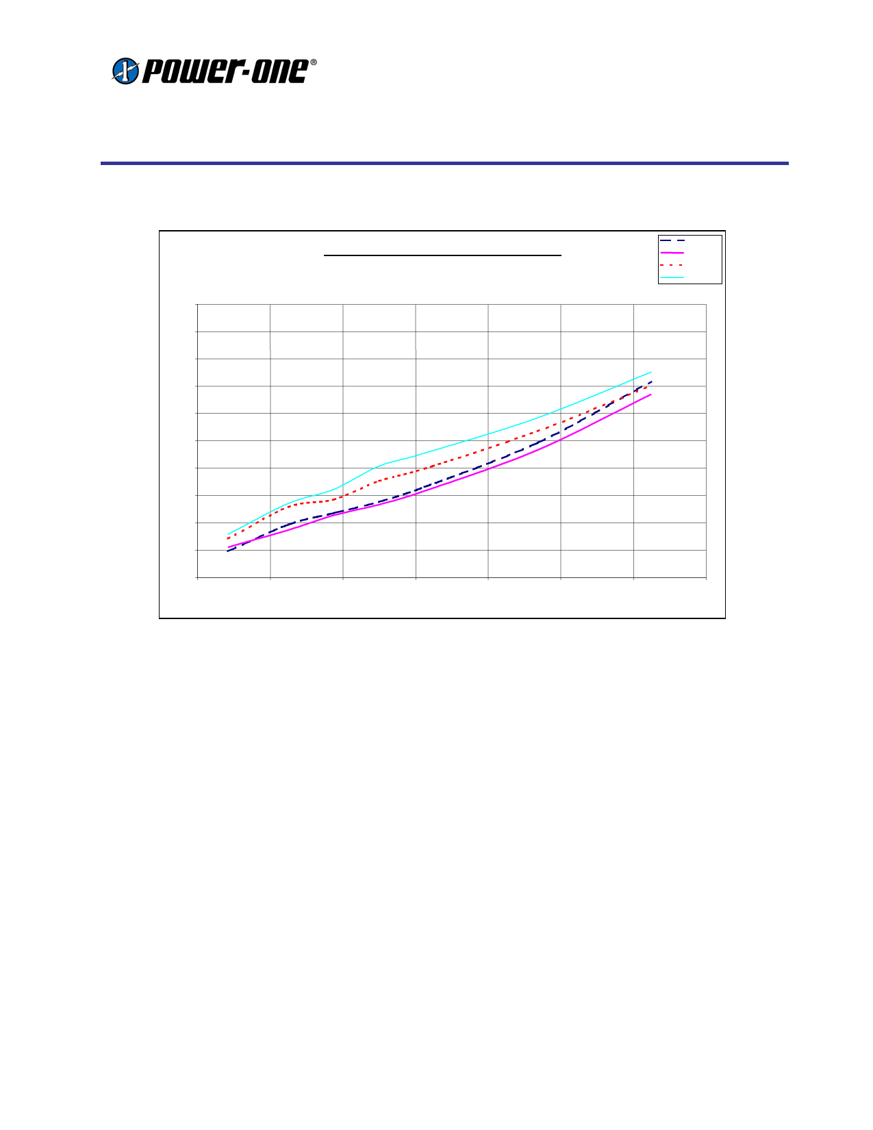
HWD15DGE Efficiency vs Output Power
90
85
80
Eff
ici 75
en
cy
(%
) 70
65
60
55
0
10
20
30
40
50
60
Output Power (W)
Figure 7. Efficiency Vs. Output Power
Vinmin
Vinnom1
Vinnom2
Vinmax
Vinmin
Vinnom1
Vinnom2
Vinmax
70
REV. JUN 27, 2003
Page 10 of 12
Share Link: 