HV857L Ver la hoja de datos (PDF) - Supertex Inc
Número de pieza
componentes Descripción
Fabricante
HV857L Datasheet PDF : 8 Pages
| |||
HV857L
Low Noise, High Voltage EL Lamp Driver IC
Features
► Audible noise reduction
► 190 VPP output voltage for higher brightness
► Single cell lithium ion compatible
► 150nA shutdown current
► Wide input voltage range 1.8V to 5.0V
► Separately adjustable lamp and converter
frequencies
► Output voltage regulation
► Split supply capability
► Available in DFN-8 and MSOP-8 packages
Applications
► Mobile cellular phones
► Keypad backlighting
► LCD backlighting
► PDAs
► Handheld wireless communication products
► Global Positioning Systems (GPS)
General Description
The Supertex HV857L is a low noise, high voltage driver
designed for driving Electroluminescent (EL) lamps of up to five
square inches. It is the low noise version of the EL lamp driver
HV857. The input supply voltage range is from 1.8V to 5.0V. The
device uses a single inductor and a minimum number of passive
components. The nominal regulated output voltage that is applied
to the EL lamp is ±95V. The chip can be enabled/disabled by
connecting the resistor on RSW-Osc to VDD/ground.
The HV857L has two internal oscillators, a switching MOSFET,
and a high voltage EL lamp driver. The frequency for the
switching MOSFET is set by an external resistor connected
between the RSW-Osc pin and the supply pin, VDD. The EL
lamp driver frequency is set by an external resistor connected
between the REL-Osc and VDD pins. An external inductor is
connected between the LX and VDD pins, or VIN for split supply
applications. A 0.003-0.1µF capacitor is connected between CS
and ground. The EL lamp is connected between the VA and VB
pins.
The switching MOSFET charges the external inductor and
discharges it into the capacitor at CS. The voltage at CS will
start to increase. Once the voltage at CS reaches a nominal
value of 95V, the switching MOSFET is turned OFF to conserve
power. The outputs VA and VB are configured as an H bridge,
and are switching in opposite states to achieve ±95V across the
EL lamp.
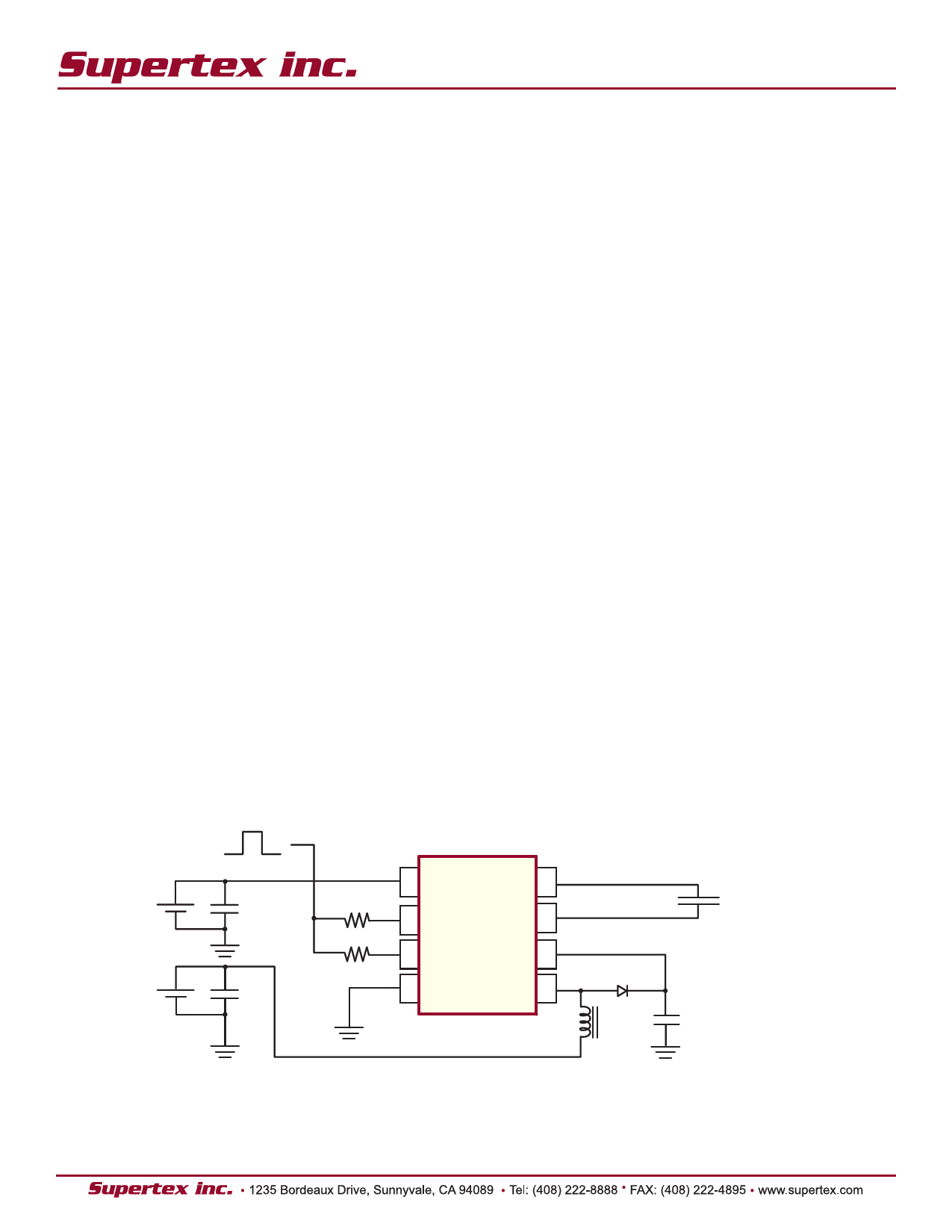
Typical Application Circuit
ON = VDD
OFF = 0
Enable Signal
+
CDD
VDD_
RSW
+
CIN
REL
VIN_
1 VDD
VA 8
2 RSW-Osc VB 7
3 REL-Osc CS 6
4 GND
LX 5
HV857LMG
EL Lamp
D
CS
LX
Share Link: 