HV853(2007) Ver la hoja de datos (PDF) - Supertex Inc
Número de pieza
componentes Descripción
Fabricante
HV853 Datasheet PDF : 7 Pages
| |||
HV853
Ordering Information
Package Options
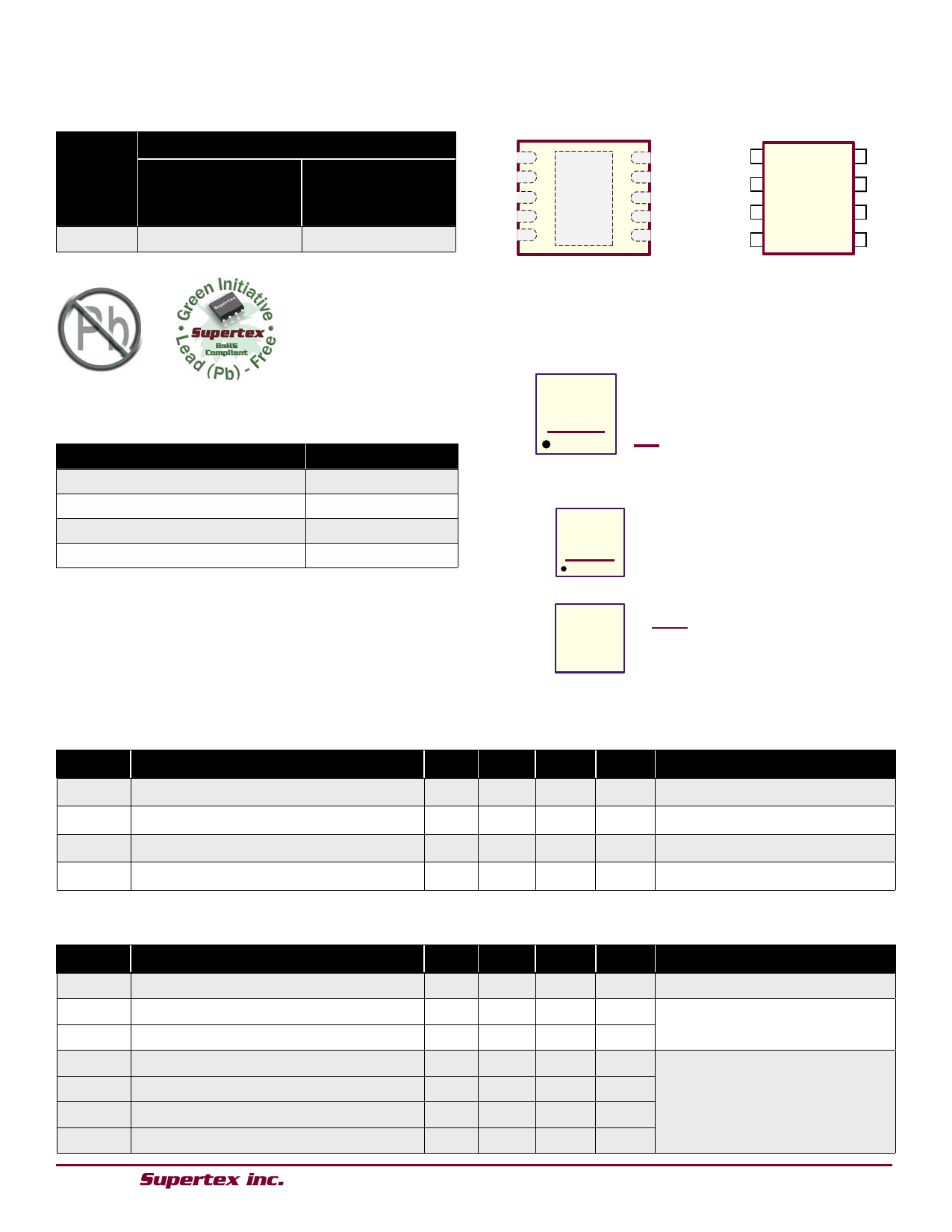
DEVICE
8-Lead DFN
3x3mm body,
0.80mm height (max),
0.65mm pitch
8-Lead MSOP
3x3mm body,
1.10mm height (max),
0.65mm pitch
HV853
HV853K7-G
HV853MG-G
-G indicates package is RoHS compliant (‘Green’)
Product Marking
H853
YWLL
Y = Last Digit of Year Sealed
W = Code for Week Sealed
L = Lot Number
= “Green” Packaging
8-Lead DFN Package (K7)
Top Marking
Absolute Maximum Ratings
H853
LLLL L = Lot Number
YY = Year Sealed
Bottom Marking WW = Week Sealed
YYWW
= “Green” Packaging
Parameter
VDD, supply voltage
Storage temperature
Value
-0.5V to 6.5V
-65°C to +150°C
8-Lead MSOP Package (MG)
Pin Configuration
Power dissipation (8-Lead DFN)
1.6W
Power dissipation (8-Lead MSOP)
300mW
Absolute Maximum Ratings are those values beyond which damage to
the device may occur. Functional operation under these conditions is not
implied. Continuous operation of the device at the absolute rating level
may affect device reliability. All voltages are referenced to device ground.
VDD 1
REL 2
EN 3
CLKIN 4
8 VA
7 VB
6 GND
5 CLKEN
VDD 1
REL 2
EN 3
CLKIN 4
8 VA
7 VB
6 GND
5 CLKEN
8-Lead DFN
(top view)
Note:
Pads are at the bottom of the package.
Center heat slug is at ground potential.
8-Lead MSOP
(top view)
Electrical Characteristics
(Over recommended operating conditions unless otherwise specified, TA = 25ºC)
Symbol Parameter
Min Typ Max Units Conditions
IDDQ
VA or VB
VA-VB
IDD
VA or VB
VA-VB
fEL
Quiescent current
Peak output voltage
Peak to peak output voltage
Operating current
Peak output voltage
Peak to peak output voltage
EL lamp frequency
trout
Output voltage rise time
t
Output voltage fall time
fout
Logic Inputs
VIL Input logic low voltage
VIH Input logic high voltage
IIL
Input logic low current
I
Input logic high current
IH
-
-
150
68 80
92
136 160 184
-
15
30
68 80
92
136 160 184
240 280 320
- 450
-
150
-
-
nA EN = 0V
V
No load
V
mA
See Figure 1
V
VDD = 3.5V
V REL = 1.5MΩ
Load = 3.3nF + 1.0kΩ
Hz
µs
1.0in2 lamp
0V to 90% of final value
µs 90% to 10% of final value
0
-
0.5
V ---
2.0
-
VDD
V ---
-
-
1.0 µA ---
-
-
1.0 µA ---
2
Share Link: 