HV831 Ver la hoja de datos (PDF) - Supertex Inc
Número de pieza
componentes Descripción
Fabricante
HV831 Datasheet PDF : 8 Pages
| |||
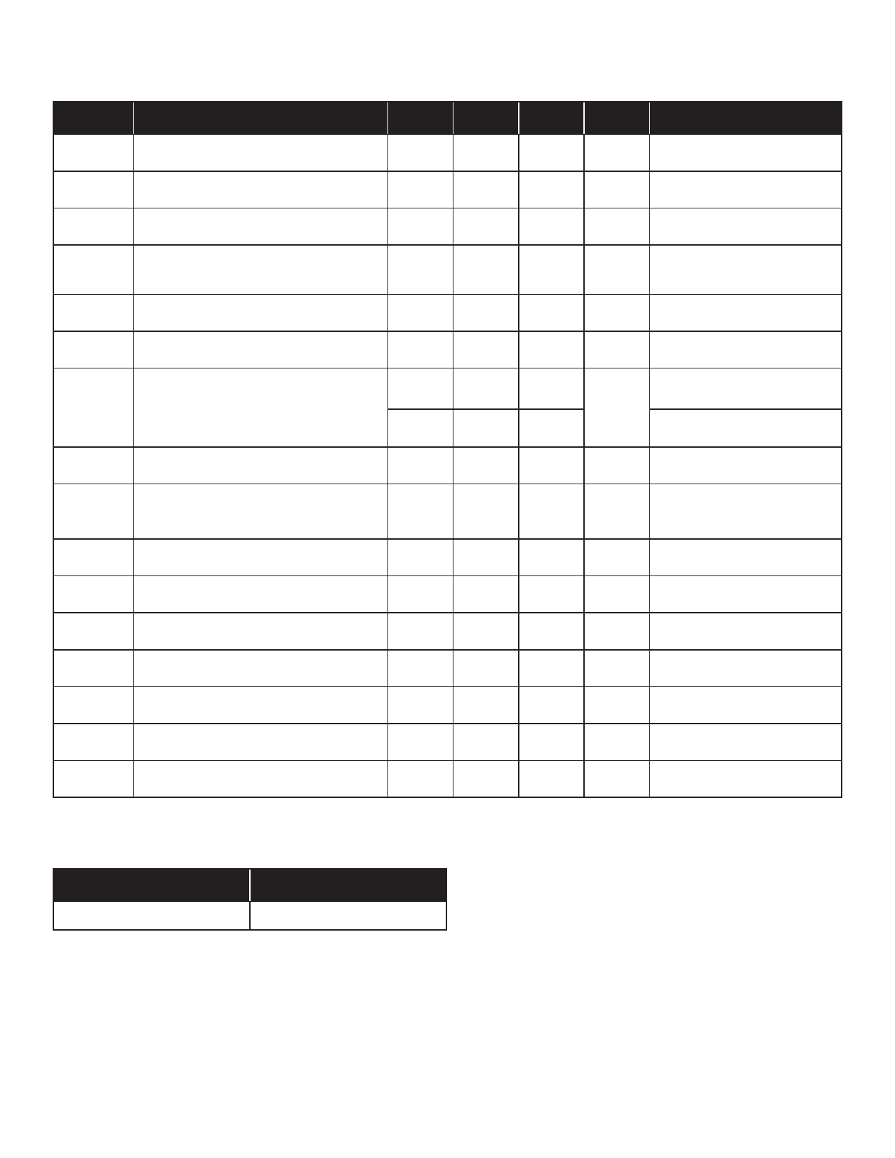
Electrical Characteristics
DC Characteristics (Over operating conditions unless otherwise specified, TA= 25°C)
Symbol Parameter
Min Typ Max
HV831
Units Conditions
RDS(ON)
On-resistance of switching transistor
6.0
Ω
I = 100mA
VDD
Input Voltage Range
2.0
5.0
V
Vcs
VDIFF
IDDQ
Output regulation voltage
72
80
88
Differential output peak to peak voltage
(EL1 to Com, EL2 to Com)
144
160
176
Quiescent VDD supply current
150
V
VDD = 2.0V to 5.0V
V
VDD = 2.0V to 5.0V
nA
C1 = C2 = 0V
IDD
IIN
VCS
V
DIFF
fEL
Input current into the VDD pin
150
Input current including inductor current
when driving both lamps
45
26.5
35
Output voltage on VCS when driving both
lamps
Differential output peak to peak voltage
across each lamp
(EL1 to Com, EL2 to Com)
67.8
135.6
VDIFF output drive frequency
214
244
274
µA
VDD = 2.0V to 5.0V
VIN = 3.0V, See Figure 1.
mA
TA = -40°C to +85°C
VIN = 3.0V, See Figure 1.
TA = +25°C
V
VIN = 3.0V. See Figure 1.
V
V = 3.0V. See Figure 1.
IN
Hz
VIN = 3.0V. See Figure 1.
fSW
Switching transistor frequency
27.4
31.2
35
kHz VIN = 3.0V. See Figure 1.
D
Switching Transistor Duty cycle
85
IIL
Input logic low current going into the
control pin
IIH
Input logic low current going into the
control pin
VEN-L
Logic input low voltage
0
89
-0.6
0.6
0.2VDD
%
µA
VDD = 2.0V to 5.8V
µA
VDD = 2.0V to 5.8V
V
VEN-H
Logic input high voltage
0.8VDD
VDD
V
Thermal Resistance
(Mounted on FR4 board, 25mm x 25mm x 1.57mm)
Package
MSOP-10
θJA
400 oC/W
3
A081005
Share Link: 