HV623 Ver la hoja de datos (PDF) - Supertex Inc
Número de pieza
componentes Descripción
Fabricante
HV623 Datasheet PDF : 10 Pages
| |||
HV623
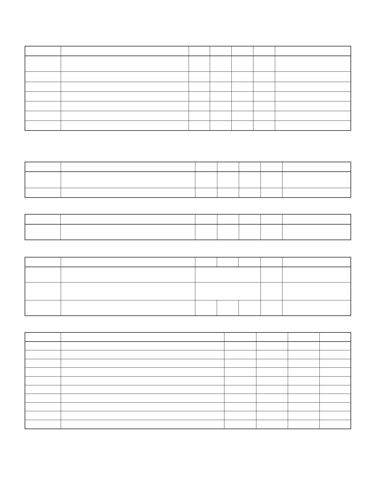
Electrical Characteristics (at TA = 25°C, over operating conditions unless otherwise specified)
Low-Voltage DC Characteristics (Digital)
Symbol
Parameter
Min Typ1 Max Units
Conditions
IDD
VDD supply current
IDDQ
Quiescent VDD supply current
IIH
High-level input current
IIL
Low-level input current
CIN2
Input capacitance (data, LC, SC, CC)
IOH
High-level output current
IOL
Low-level output current
Notes
1. All typical values are at VDD = 5.0V.
2. Guaranteed by design.
12
20
mA
fSC = 10MHz
fCC = 8MHz
100
µA
All VIN = 0V, VDD = max
1.0
50
µA
VIH = VDD
-1.0 -50
µA
VIL = 0V
15
pF
VIN = 0V, f = 1MHz
-2
mA
VDD = 4.5V
2
mA
VDD = 4.5V
Low-Voltage DC Characteristics (Analog)
Symbol
Parameter
IDD
VDD supply current
IDDQ
Quiescent VDD supply current
Min Typ Max Units
Conditions
100
µA
fSC =10MHz
fCC = 8MHz
100
µA
All VIN = 0V, VDD = max
High-Voltage Bias Circuit for Output Variation Control
Symbol
Parameter
Min Typ Max Units
Conditions
IPP
VPP supply current for bias circuit
2
mA
Depending on external
bias circuit, see Table 1.
High-Voltage DC Characteristics
Symbol
Parameter
IAOH
High-voltage analog output source current
Min Typ Max Units
See Performance Curves mA
IAOL
High-voltage analog output sink current
See Performance Curves mA
∆VO
Maximum delta voltage between high voltage outputs
of the same level
±0.2
V
Conditions
VPP = 80V
See test circuit
VPP = 80V, VDD = 4.5V
VAO = 2V
At all gray levels
Recommended Operating Conditions
Symbol
Parameter
Min
Typ
VDD
VDD
VIH
VIL
VBIAS
VCTL
VPP
VR
fSC
TA
Low-voltage digital supply voltage
Low-voltage analog supply voltage
High-level input voltage (analog and digital)
Low-level input voltage (analog and digital)
IPP control circuit bias voltage
IPP control circuit control voltage
High-voltage supply
Ramp voltage
Shift clock operating frequency (at VDD = 5.5V)
Operating free-air temperature
4.5
5.0
4.5
5.0
VDD -1
0
-2
0
0
-0.3
0
-40
Notes:
Power-up sequence should be the following:
1. Connect ground. 2. Apply VDD. 3. Set all inputs (Data, CLK, Enable, etc.) to a known state.
Power-down sequence should be the reverse of the above.
4. Apply VPP.
Max
5.5
5.5
VDD
1
2
80
VPP -2
10.2
70
Units
V
V
V
V
V
V
V
V
MHz
°C
12-123
Share Link: 