HV518 Ver la hoja de datos (PDF) - Supertex Inc
Número de pieza
componentes Descripción
Fabricante
HV518 Datasheet PDF : 8 Pages
| |||
HV518
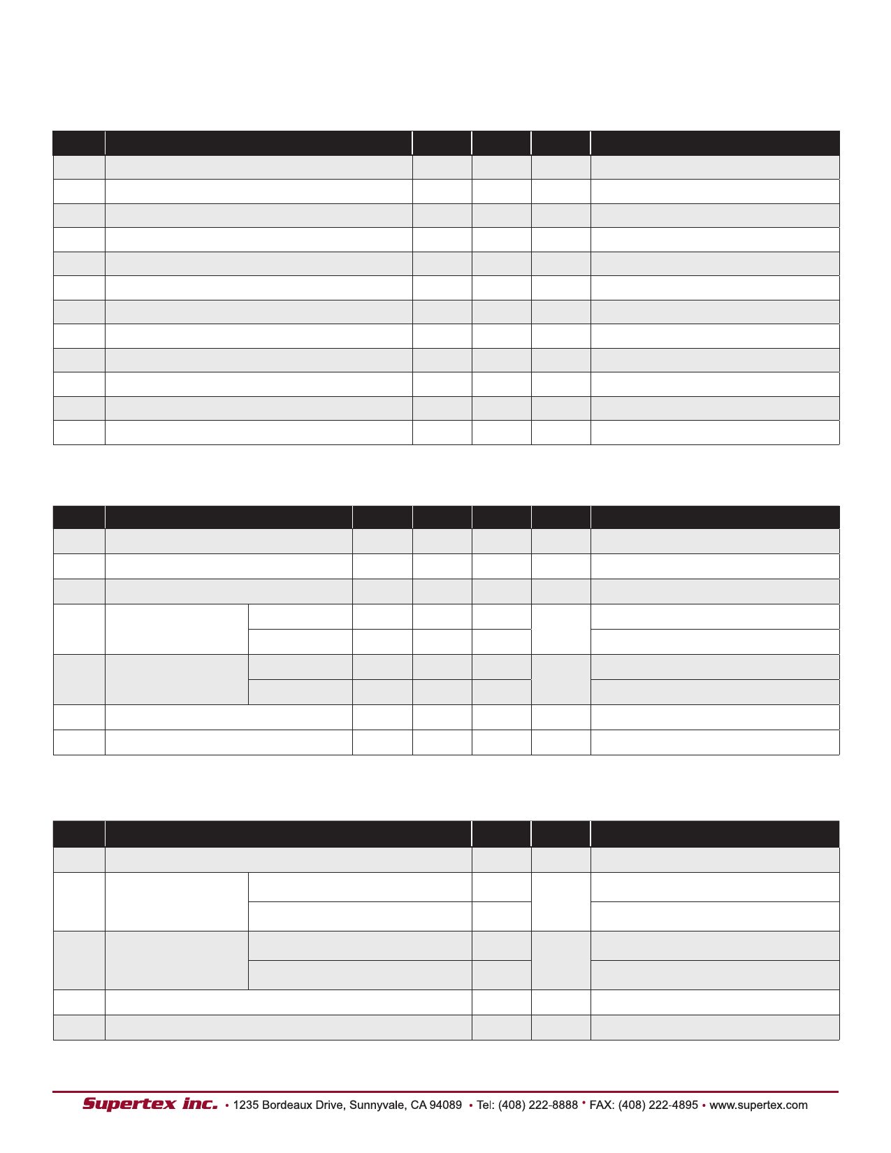
Recommended Operating Conditions (TA = 25°C, unless otherwise noted)
Sym Parameter
Min Max Unit Conditions
V
DD
VPP
VIH
V
IL
IOH
IOL
fCLK
tw(CKH)
tw(CKL)
tsu
th
TA
Logic supply voltage
High voltage supply
High-level input voltage
Low-level input voltage
High-level output current
Low-level output current
Clock frequency
Pulse duration, clock high
Pulse duration, clock low
Setup time, data before clock
Hold time, data after clock
Operating free-air temperature
4.5
5.5
V ---
8.0
80
V ---
3.5
-
V VDD = 4.5V, See Figure 3
-
1.0
V V = 4.5V, See Figure 3
DD
-25
-
mA ---
-
2.0
mA ---
-
6.0
MHz VDD = 4.5V, See Figure 3
83
-
ns VDD = 4.5V
83
-
ns VDD = 4.5V
75
-
ns VDD = 4.5V
75
-
ns VDD = 4.5V
-40
85
°C ---
Electrical Characteristics
(over recommended ranges of operating free-air temperature and VDD. Unless otherwise noted, VPP = 80V)
Sym Parameter
Min
Typ
Max Units Conditions
IDD
Supply current
-
-
10
mA VDD = 5.0V, fCH = 6.0 MHz
IDDQ Quiescent supply current
-
-
0.5
mA VDD = 5.5V, VIN = 0V
IPPQ Quiescent supply current
-
-
100
µA ---
VOH
HVIN operating
current
HV output
70
-
-
Serial output 4.5
4.9
5.0
V
IOH = -25mA
VDD = 5.0V, IOH = -20µA
VOL
LVIN operating
current
HV output
-
Serial output
-
-
5.0
0.06 0.8
V
IOL = 1.0mA
I = 20µA
OL
IIH
Logic input current high
-
0.1
1.0
µA
VIH = VDD
IIL
Logic input current low
-
-0.1 -1.0
µA VIL = 0V
Note: The total number of ON outputs times the duty cycle must not exceed the allowable package power disspation.
Switching Characteristics (VPP = 80V, CL = 50pF, TA = 25°C, unless otherwise noted)
Sym Parameter
Max Unit Conditions
td
Delay time, clock to data output
Turn-on time when
tDHL high voltage is
enabled
from latch enable
from strobe
Delay time,
tDLH high-to-low-level,
HV output
from latch enable
from strobe
tTHL Transition time, high-to-low-level, HV output
tTLH Transition time, low-to-high-level, HV output
600
ns VDD = 4.5V, CL = 15pF, See Figure 1
1.5
µs
VDD = 4.5V, See Figure 2
1.0
VDD = 4.5V, See Figure 3
1.5
µs
VDD = 4.5V, See Figure 2
1.0
VDD = 4.5V, See Figure 3
3.0
µs VDD = 4.5V, See Figure 3
2.5
µs VDD = 4.5V, See Figure 3
3
Share Link: 