HT56R66 Ver la hoja de datos (PDF) - Holtek Semiconductor
Número de pieza
componentes Descripción
Fabricante
HT56R66 Datasheet PDF : 104 Pages
| |||
HT56R66/HT56R666
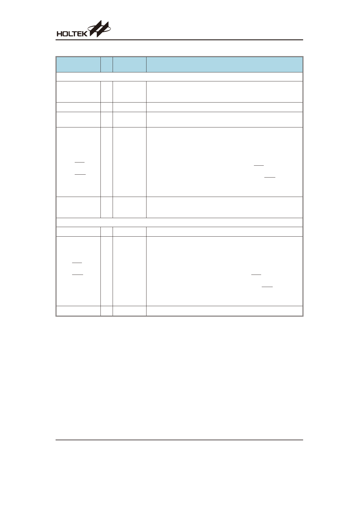
The following tables depict the device dependent pins.
Pin Name
I/O
Configuration
Option
Description
HT56R66
PC0~PC7
Bidirectional 8-bit input/output port. Software instructions determine the
I/O
¾
CMOS output, Schmitt trigger input with or without pull-high resistor (de-
termined by PCPU register control bit)
VMAX
I
¾
IC maximum voltage, connect to VDD, VLCD1 or V1
VLCD1/VLCD2/V1,
C1, C2
¾
¾
LCD Voltage pump pins for C-type biasing.
For R-type biasing only pin VLCD1 are used.
SEG0~SEG9
O
SEG10/SDO
O
SEG11/SDI/SDA I/O
SEG12/SCK/SCL I/O
SEG13/SCS
I/O
SEG14/PCLK
O
SEG15/PINT
I/O
SEG16~SEG47
O
SIM
PINT
SEG0~SEG47 are LCD driver outputs for LCD panel segments.
SEG10 is pin-shared with the SPI bus data output line, SDO.
SEG11 is pin-shared with the SPI bus data input line, SDI and the I2C Bus
data line SDA.
SEG12 is pin-shared with the SPI bus clock line, SCK and the I2C Bus
clock line SCL.
SEG13 is pin-shared with the SPI bus select line, SCS.
SEG14 is pin-shared with the Peripheral Clock line, PCLK.
SEG15 is pin-shared with the Peripheral Interrupt line, PINT.
The SEG0~SEG23 lines can be can be chosen to be either segment driv-
ers or CMOS outputs using control bits in the LCD control registers.
COM0~COM2
COM3/SEG48
O
COM0~COM2 are the LCD common outputs. A bit in the LCD Control
¾
Register determines if pin COM3/SEG48 is configured as a segment
driver or as a common output driver.
HT56R666
VLCD
I
SEG0/SDO
O
SEG1/SDI/SDA I/O
SEG2/SCK/SCL I/O
SEG3/SCS
I/O
SEG4/PCLK
O
SEG5/PINT
I/O
SEG6~SEG47
O
COM15/SEG48~ O
COM8/SEG55
COM0~COM7
O
¾
SIM
PINT
¾
LCD bias pin - must less than or equal to VDD
SEG0~SEG47 are LCD driver outputs for LCD panel segments.
SEG0 is pin-shared with the SPI bus data output line, SDO.
SEG1 is pin-shared with the SPI bus data input line, SDI and the I2C Bus
data line SDA.
SEG2 is pin-shared with the SPI bus clock line, SCK and the I2C Bus clock
line SCL.
SEG3 is pin-shared with the SPI bus select line, SCS.
SEG4 is pin-shared with the Peripheral Clock line, PCLK.
SEG5 is pin-shared with the Peripheral Interrupt line, PINT.
The SEG0~SEG23 lines can be can be chosen to be either segment driv-
ers or CMOS outputs using control bits in the LCD control registers.
COM0~COM7 are the LCD common outputs.
Note: The Pin Description tables represents the largest package type available, therefore some of the pins and func-
tions may not be available on smaller package types.
Absolute Maximum Ratings
Supply Voltage ...........................VSS-0.3V to VSS+6.0V
Input Voltage..............................VSS-0.3V to VDD+0.3V
IOL Total ................................................................80mA
Total Power Dissipation .....................................500mW
Storage Temperature ............................-50°C to 125°C
Operating Temperature...........................-40°C to 85°C
IOH Total..............................................................-80mA
Note: These are stress ratings only. Stresses exceeding the range specified under ²Absolute Maximum Ratings² may
cause substantial damage to the device. Functional operation of this device at other conditions beyond those listed
in the specification is not implied and prolonged exposure to extreme conditions may affect device reliability.
Rev. 1.40
5
May 11, 2012
Share Link: 