HT49C30-1 Ver la hoja de datos (PDF) - Holtek Semiconductor
Número de pieza
componentes Descripción
Fabricante
HT49C30-1 Datasheet PDF : 43 Pages
| |||
HT49R30A-1/HT49C30-1/HT49C30L
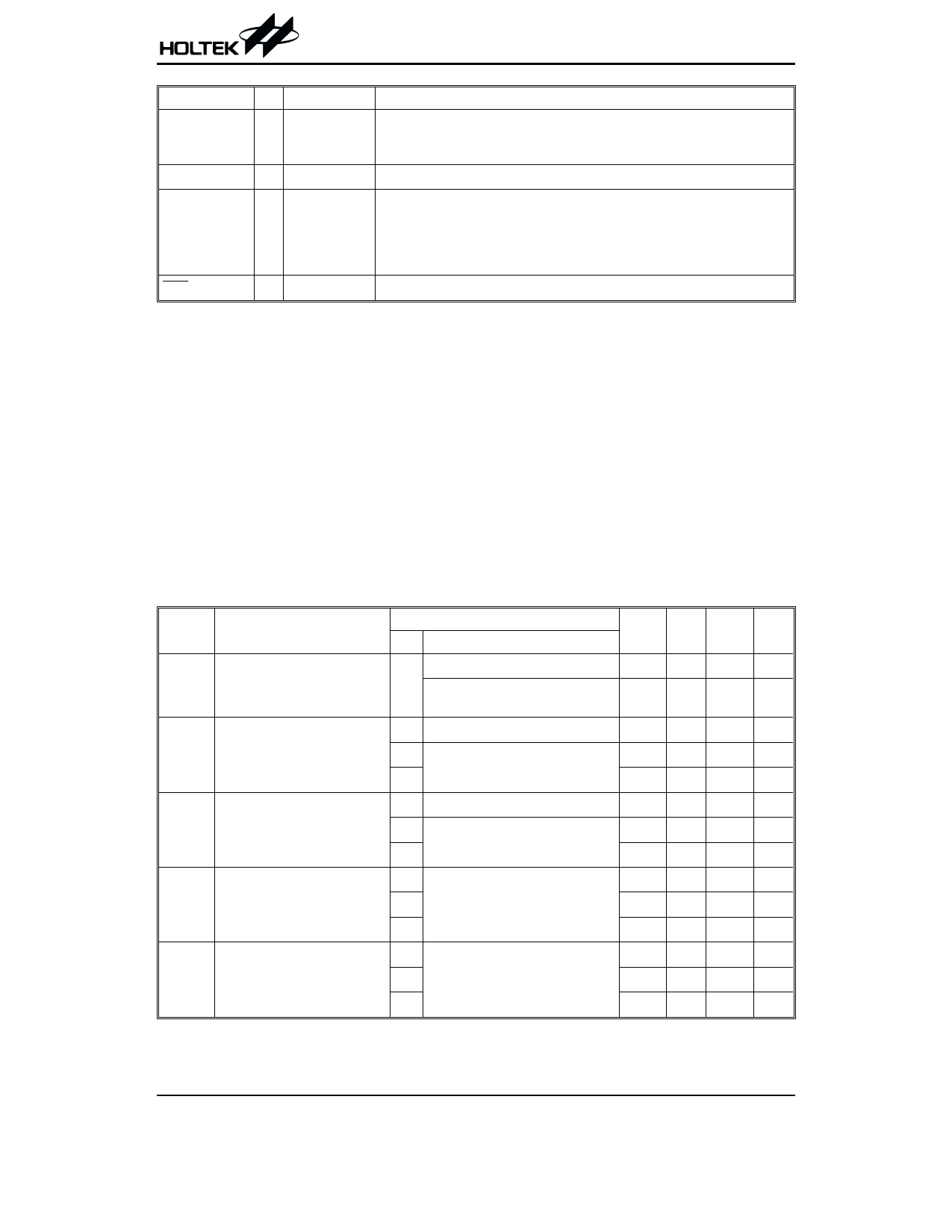
Pad Name
OSC4
OSC3
VDD
OSC2
OSC1
RES
I/O Options
Description
O
I
RTC or
System Clock
Real time clock oscillators. OSC3 and OSC4 are connected to a 32768Hz
crystal oscillator for timing purposes or to a system clock source (depending
on the options).
¾
¾
Positive power supply
OSC1 and OSC2 are connected to an RC network or a crystal (by options)
O
I
for the internal system clock. In the case of RC operation, OSC2 is the output
Crystal or RC terminal for 1/4 system clock.
The system clock may come from the RTC oscillator. If the system clock co-
mes from RTCOSC, these two pins can be floating.
I
¾
Schmitt trigger reset input, active low
Absolute Maximum Ratings
Supply Voltage..................................VSS-0.3V to 5.5V*
Storage Temperature ............................-50°C to 125°C
Operating Temperature ...........................-40°C to 85°C
Supply Voltage ................................VSS-0.3V to 2.2V**
Input Voltage..............................VSS-0.3V to VDD+0.3V
Note: These are stress ratings only. Stresses exceeding the range specified under ²Absolute Maximum Ratings² may
cause substantial damage to the device. Functional operation of this device at other conditions beyond those
listed in the specification is not implied and prolonged exposure to extreme conditions may affect device reliabil-
ity.
²*² For HT49R30A-1/HT49C30-1
²**² For HT49C30L
D.C. Characteristics
VDD=1.5V for HT49C30L, VDD=3V & VDD=5V for HT49R30A-1 and HT49C30-1
Symbol
Parameter
VDD
Operating Voltage
Test Conditions
VDD
Conditions
for HT49C30L
¾ LVR disable
(for HT49R30A-1/HT49C30-1)
IDD1
Operating Current
(Crystal OSC)
1.5V No load, fSYS=455kHz
3V
No load, fSYS=4MHz
5V
IDD2
Operating Current
(RC OSC)
1.5V No load, fSYS=400kHz
3V
No load, fSYS=4MHz
5V
IDD3
Operating Current
(fSYS=32768Hz)
1.5V
3V No load
5V
ISTB1
Standby Current
(*fS=T1)
1.5V
3V
No load, system HALT,
LCD off at HALT
5V
Ta=25°C
Min. Typ. Max. Unit
1.2 ¾ 2.2 V
2.2 ¾ 5.5 V
¾ 60 100 mA
¾
1
2 mA
¾
3
5 mA
¾ 50 100 mA
¾
1
2 mA
¾
3
5 mA
¾ 2.5
4
mA
¾ 0.3 0.6 mA
¾
2
4 mA
¾ 0.1 0.5 mA
¾¾
1
mA
¾¾
2
mA
Rev. 1.10
5
September 25, 2002
Share Link: 