HT46R52 Ver la hoja de datos (PDF) - Holtek Semiconductor
Número de pieza
componentes Descripción
Fabricante
HT46R52 Datasheet PDF : 42 Pages
| |||
HT46R51/HT46R52
Instruction
TABRDC [m]
TABRDL [m]
b10 b9
P10 P9
1
1
Table Location
b8
b7
b6
b5
b4
b3
b2
b1
b0
P8 @7 @6 @5 @4 @3 @2 @1 @0
1
@7 @6 @5 @4 @3 @2 @1 @0
Table Location
Note:
b10~b0: Table location bits
P10~P8: Current program counter bits
@7~@0: Table pointer bits
For the Ht46R51, since the program counter is 10 bits wide (b0~b9), the b10 column in the table are not appli-
cable
For the HT46R52, since the program counter is 11 bits wide (b0~b10)
Stack Register - STACK
This is a special part of the memory which is used to
save the contents of the program counter only. The
stack is organized into 6 levels and is neither part of the
data nor part of the program space, and is neither read-
able nor writeable. The activated level is indexed by the
stack pointer (SP) and is neither readable nor writeable.
At the state of a subroutine call or an interrupt acknowl-
edgment, the contents of the program counter are
pushed onto the stack. At the end of the subroutine or an
interrupt routine, signaled by a return instruction (RET or
RETI), the program counter is restored to its previous
value from the stack. After a chip reset, the SP will point
to the top of the stack.
If the stack is full and a non-masked interrupt takes
place, the interrupt request flag will be recorded but the
acknowledge signal will be inhibited. When the stack
pointer is decremented (by RET or RETI), the interrupt is
serviced. This feature prevents stack overflow, allowing
the programmer to use the structure more easily. If the
stack is full and a ²CALL² is subsequently executed,
stack overflow occurs and the first entry will be lost (only
the most recent 6 return addresses are stored).
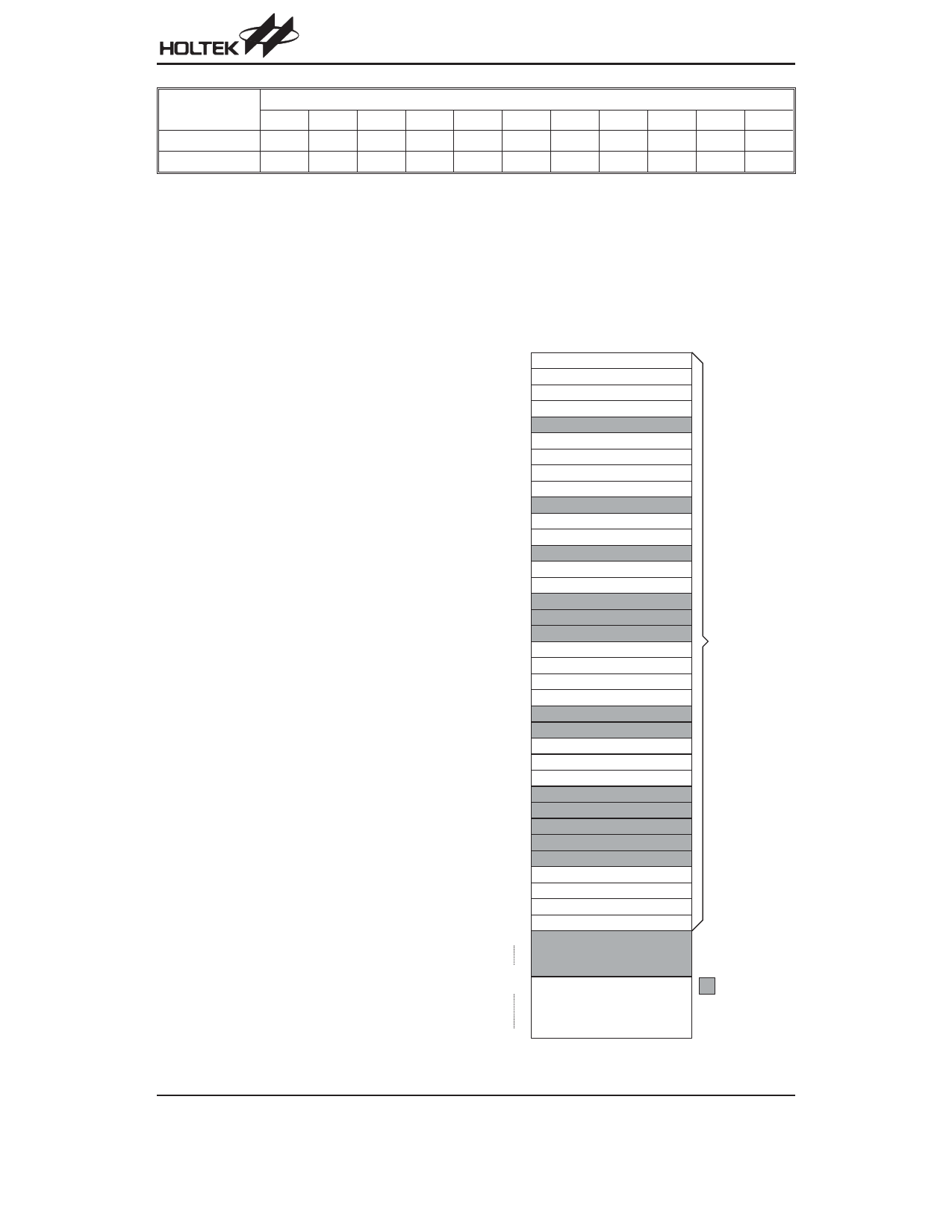
Data Memory - RAM
The data memory (RAM) is designed with 111´8 bits
and is divided into two functional groups, namely; spe-
cial function registers (23´8 bits) and general purpose
data memory (88´8bit) most of which are read-
able/writable, although some are read only. Of the two
types of functional groups, the special function registers
consist of an Indirect addressing register 0 (00H), a
Memory pointer register 0 (MP0;01H), an Indirect ad-
dressing register 1 (02H), a Memory pointer register 1
(MP1;03H), an Accumulator (ACC;05H), a Program
counter lower-order byte register (PCL;06H), a Table
pointer (TBLP;07H), a Table higher-order byte register
(TBLH;08H), a Status register (STATUS;0AH), an Inter-
rupt control register (INTC;0BH), a Timer/Event Counter
(TMR:0DH), a Timer/Event Counter control register
(TMRC;0EH), PWM data register (PWM;1AH), the A/D
00H
In d ir e c t A d d r e s s in g R e g is te r 0
01H
M P0
02H
In d ir e c t A d d r e s s in g R e g is te r 1
03H
M P1
04H
05H
ACC
06H
PCL
07H
TB LP
08H
TB LH
09H
0A H
STATU S
0B H
IN T C
0C H
0D H
TM R
0E H
TM R C
0FH
10H
11H
12H
PA
13H
PAC
14H
PB
15H
PBC
16H
PC
17H
PCC
18H
PD
19H
PDC
1A H
PW M
1B H
1C H
1D H
1E H
1FH
20H
ADRL
21H
ADRH
22H
ADCR
23H
ACSR
24H
S p e c ia l P u r p o s e
D ATA M EM O R Y
27H
28H
G e n e ra l P u rp o s e
:U nused
D a ta M e m o ry
R e a d a s "0 0 "
(8 8 B y te s )
7FH
RAM Mapping
Rev. 1.40
7
July 12, 2005
Share Link: 