HT46R01B-1 Ver la hoja de datos (PDF) - Holtek Semiconductor
Número de pieza
componentes Descripción
Fabricante
HT46R01B-1 Datasheet PDF : 71 Pages
| |||
HT46R01B-1/HT46R01N-1
HT48R01B-1/HT48R01N-1
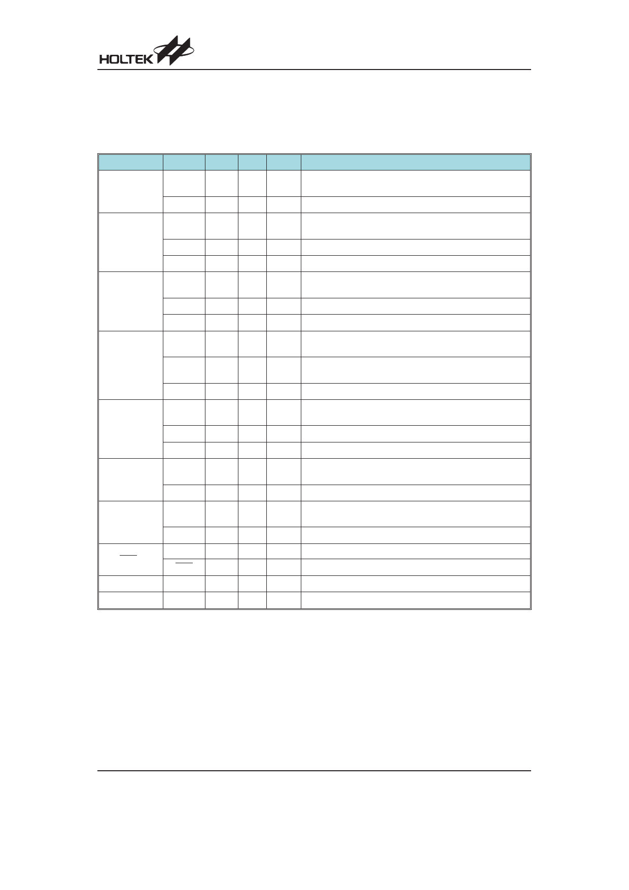
Pin Description
The function of each pin is listed in the following tables, however the details behind how each pin is configured is con-
tained in the other individual peripheral function sections.
HT46R01B-1
Pin Name Function OPT I/T O/T
Description
PA0/AN0
PA0
PAPU
PAWK
ST
CMOS General purpose I/O. Register enabled pull-up and wake-up.
AN0 ADCR OPAI ¾ Analog to Digital Converter channel input 0
PA1/PFD/AN1
PA1
PFD
PAPU
PAWK
ST
CMOS General purpose I/O. Register enabled pull-up and wake-up.
CTRL0 ¾ CMOS PFD output
AN1 ADCR ¾ OPAO Analog to Digital Converter channel input 1
PA2/TC0/AN2
PA2
PAPU
PAWK
ST
CMOS General purpose I/O. Register enabled pull-up and wake-up.
TC0 TMR0C ST
¾ External Timer 0 clock input
AN2 ADCR ¾ OPAO Analog to Digital Converter channel input 2
PA3
PAPU
PAWK
ST
CMOS General purpose I/O. Register enabled pull-up and wake-up.
PA3/INT/AN3
INT
INTC0
CTRL1
ST
¾ External interrupt input
AN3 ADCR OPAI ¾ Analog to Digital Converter channel input 3
PA4/TC1/PWM
PA4
PAPU
PAWK
ST
CMOS General purpose I/O. Register enabled pull-up and wake-up.
TC1 TMR1C ST
¾ External Timer 1 clock input
PWM CTRL0 ¾ CMOS PWM output
PA5/OSC2
PA5
PAPU
PAWK
ST
CMOS General purpose I/O. Register enabled pull-up and wake-up.
OSC2 CO ¾ OSC Oscillator pin
PA6/OSC1
PA6
OSC1
PAPU
PAWK
ST
CMOS General purpose I/O. Register enabled pull-up and wake-up.
CO OSC ¾ Oscillator pin
PA7/RES
PA7
RES
PAWK ST NMOS General purpose I/O. Register enabled wake-up.
CO ST
¾ Reset input
VDD
VDD
¾ PWR ¾ Power supply
VSS
VSS
¾ PWR ¾ Ground
Note:
OPT: Optional by configuration option (CO) or register option
I/T: Input type
O/T: Output type
CO: Configuration option
ST: Schmitt Trigger input
AN: analog input;
CMOS: CMOS output
NMOS: NMOS output
OSC: Oscillator pin
PWR: Power
*: AVDD is the ADC power supply and is bonded together internally with VDD while AVSS is the ADC ground
pin and is bonded together internally with VSS.
Rev.1.00
3
June 9, 2011
Share Link: 