HT48R062 Ver la hoja de datos (PDF) - Holtek Semiconductor
Número de pieza
componentes Descripción
Fabricante
HT48R062 Datasheet PDF : 31 Pages
| |||
HT48R062/HT48C062
Input/Output Ports
There are up to 11 bidirectional input/output lines in the
microcontroller labeled with port names PA and PB,
which are mapped to the data memory of [12H] and
[14H] respectively. All of these I/O ports can be used for
input and output operations. For input operation, these
ports are non-latching, that is, the inputs must be ready
at the T2 rising edge of instruction ²MOV A,[m]² (m=12H
or 14H). For output operation, all the data is latched and
remains unchanged until the output latch is rewritten.
Each I/O line has its own control register (PAC, PBC) to
control the input/output configuration. With this control
register, CMOS output or Schmitt trigger input with or
without pull-high resistor structures can be reconfigured
dynamically (i.e. on-the-fly) under software control. To
function as an input, the corresponding latch of the con-
trol register must write ²1². The input source also de-
pends on the control register. If the control register bit is
²1², the input will read the pad state. If the control regis-
ter bit is ²0², the contents of the latches will move to the
internal bus. The latter is possible in the ²read-modify-
write² instruction.
For output function, CMOS is the only configuration.
These control registers are mapped to locations 13H
and 15H.
After a chip reset, these input/output lines remain at high
levels or floating state (dependent on pull-high options).
Each bit of these input/output latches can be set or
cleared by ²SET [m].i² and ²CLR [m].i² (m=12H or 14H)
instructions.
Some instructions first input data and then follow the
output operations. For example, ²SET [m].i², ²CLR
[m].i², ²CPL [m]², ²CPLA [m]² read the entire port states
into the CPU, execute the defined operations
(bit-operation), and then write the results back to the
latches or the accumulator.
Each line of Port A has the capability of waking-up the
device. The highest 5-bit of Port B are not physically im-
plemented; on reading them a ²0² is returned whereas
writing then results in a no-operation. See Application
note.
There are pull-high options available for PA and PB.
Once the pull-high option is selected, I/O lines have
pull-high resistors. Otherwise, the pull-high resistors are
absent. It should be noted that a non-pull-high I/O line
operating in input mode will cause a floating state.
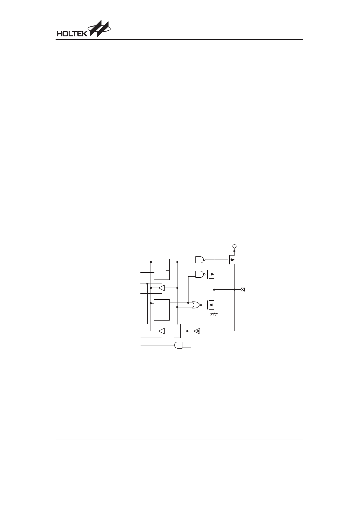
D a ta B u s
W r ite C o n tr o l R e g is te r
C h ip R e s e t
R e a d C o n tr o l R e g is te r
W r ite D a ta R e g is te r
R e a d D a ta R e g is te r
S y s te m W a k e -u p
( P A o n ly )
V DD
C o n tr o l B it P u ll- h ig h
D
Q
CK Q
S
D a ta B it
D
Q
CK Q
S
M
U
X
W a k e - u p O p tio n
Input/Output Ports
P A 0~P A 7
P B 0~P B 2
Rev. 1.21
10
December 30, 2008
Share Link: 