HT48R01 Ver la hoja de datos (PDF) - Holtek Semiconductor
Número de pieza
componentes Descripción
Fabricante
HT48R01 Datasheet PDF : 38 Pages
| |||
HT48R01/HT48R02/HT48R03
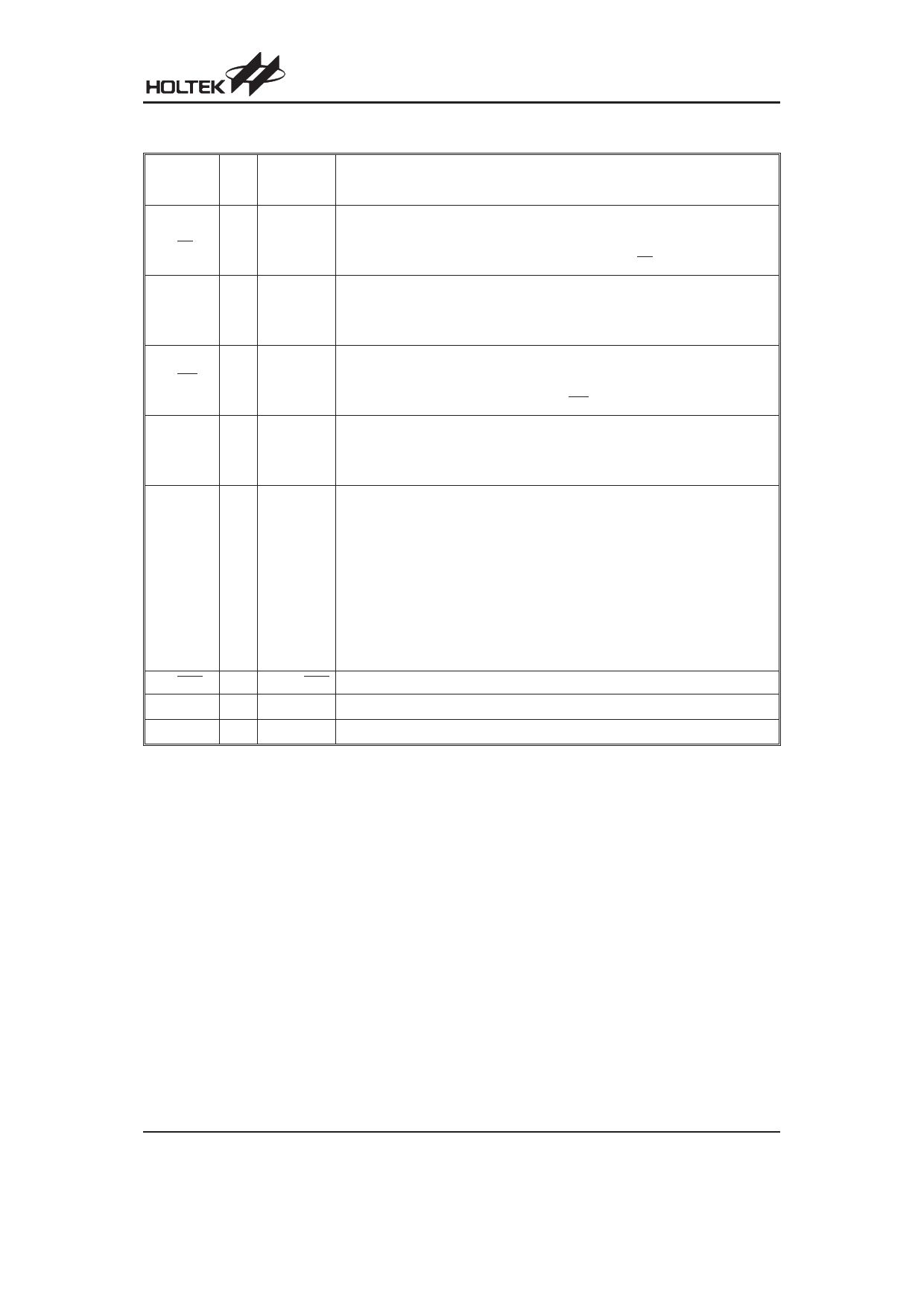
Pin Description
Configura-
Pin Name I/O
tion
Options
Description
PA0/BZ
PA1/BZ
I/O
Bidirectional 2-line I/O. Each pin can be setup as a wake-up input using a soft-
¾
ware register. Software instructions determine if each pin is a CMOS output or a
Schmitt trigger input. Pull-high resistors can be connected using a pull-high soft-
ware register. PA0/PA1 are pin-shared with the BZ and BZ buzzer function pins.
PA2/TMR0 I/O
Bidirectional single line I/O. PA2 can be setup as a wake-up input using a soft-
¾
ware register. Software instructions determine if the pin is a CMOS output or
Schmitt trigger input. A pull-high resistor can be connected using a pull-high soft-
ware register. This line is pin-shared with the Timer/event 0 counter input.
PA3/INT
I/O
Bidirectional single line I/O. PA3 can be setup as a wake-up input using a soft-
¾
ware register. Software instructions determine if the pin is a CMOS output or
Schmitt trigger input. A pull-high resistor can be connected using a pull-high soft-
ware register. This line is pin-shared with INT.
PA4/TMR1 I/O
Bidirectional single line I/O. PA4 can be setup as a wake-up input using a soft-
¾
ware register. Software instructions determine if the pin is a CMOS output or
Schmitt trigger input. A pull-high resistor can be connected using a pull-high soft-
ware register. This line is pin-shared with the Timer/event counter 1 input.
OSC1/PA6
OSC2/PA5
Bidirectional 2-line I/O and oscillator pins. If configured as I/Os, software instruc-
tions determine if each pin is a CMOS output or a Schmitt trigger input. Pull-high
resistors can be connected using a pull-high software register. A configuration
option determines the choice of oscillator mode and I/O function. The four oscilla-
tor modes are:
I/O
RC, Crystal, 1. Internal RC OSC: both pins configured as I/Os
RTC or I/O 2. External crystal OSC: both pins configured as OSC1/OSC2
3. Internal RC + RTC OSC: both pins configured as OSC2, OSC1.
4. External RC OSC+PA5: PA6 configured as OSC1 pin, PA5 configured as I/O
Note: When the system clock is sourced from the internal RC OSC, there are 3
frequency options ® 12MHz, 8MHz and 4MHz.
PA7/RES
I PA7 or RES Active low schmitt trigger reset input or PA7 input.
VDD
¾
¾
Positive power supply
VSS
¾
¾
Negative power supply, ground
* All pull-high resistors are controlled by an register option bit.
Absolute Maximum Ratings
Supply Voltage ...........................VSS-0.3V to VSS+6.0V
Input Voltage..............................VSS-0.3V to VDD+0.3V
IOL Total ..............................................................150mA
Total Power Dissipation .....................................500mW
Storage Temperature ............................-50°C to 125°C
Operating Temperature...........................-40°C to 85°C
IOH Total............................................................-100mA
Note: These are stress ratings only. Stresses exceeding the range specified under ²Absolute Maximum Ratings² may
cause substantial damage to the device. Functional operation of this device at other conditions beyond those listed
in the specification is not implied and prolonged exposure to extreme conditions may affect device reliability.
Rev. 1.00
3
December 20, 2006
Share Link: 