HT0610 Ver la hoja de datos (PDF) - Holtek Semiconductor
Número de pieza
componentes Descripción
Fabricante
HT0610 Datasheet PDF : 22 Pages
| |||
HT0610
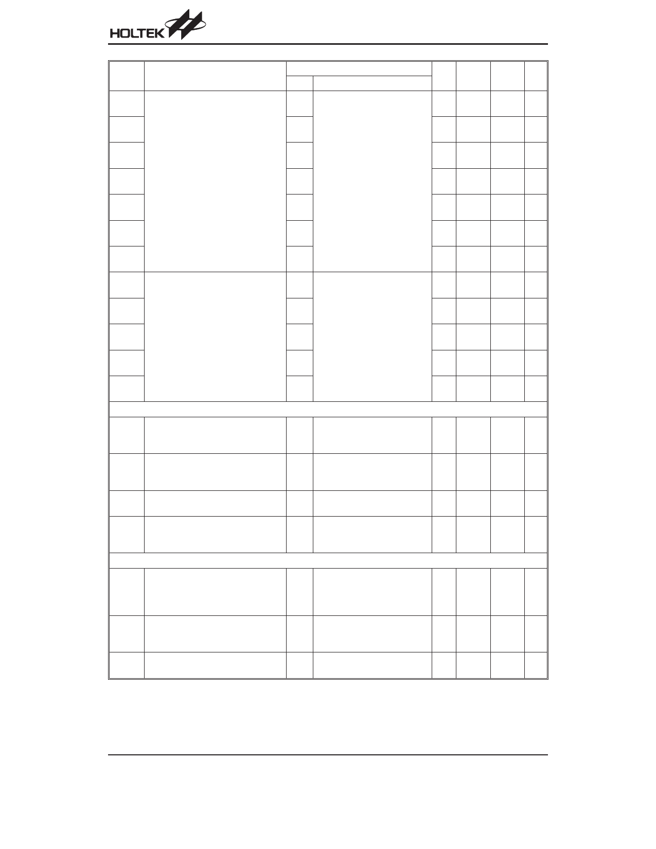
Symbol
Parameter
Test Conditions
VDD
Conditions
Min. Typ. Max. Unit
VLL6
2.4V~
3.5V
¾ VR
¾V
VLL5
2.4V~
3.5V
¾ 6/7´VR ¾ V
VLL4
2.4V~
3.5V
¾ 5/7´VR ¾ V
DUM2
2.4V~ 1/7 bias ratio, voltage divider
3.5V enable, regulator enable
¾
4/7´VR
¾
V
DUM1
2.4V~
3.5V
¾ 3/7´VR ¾ V
VLL3
2.4V~
3.5V
¾ 2/7´VR ¾ V
VLL2
2.4V~
3.5V
¾ 1/7´VR ¾ V
VLL6
2.4V~
3.5V
0.5´
¾
VCCA1
VCCA1
VLL5
2.4V~
3.5V
0.5´
¾
VCCA1
VCCA1
VLL4
2.4V~ External voltage generator, 0.5´
3.5V internal voltage divider disable VCCA1
¾
VCCA1
VLL3
2.4V~
3.5V
vss ¾
0.5´
VCCA1
VLL2
2.4V~
3.5V
vss ¾
0.5´
VCCA1
Output Current
IOH
Output High Current Source from
Pins D0~D7, ICON1~ICON4, IBP
and OSC2
2.4V~
3.5V
VOUT=VDD-0.1V
¾ 1.5
¾ mA
IOL
Output Low Current Drain by
D0~D7, ICON1~ICON4, IBP
OSC2
Pins
and
2.4V~
3.5V
VOUT=0.1V
¾
5
¾ mA
IOZ
Output Tri-state Current Drain 2.4V~
Source at Pins D0~D7 and OSC2 3.5V
¾
-1 ¾
1 mA
IIL/IIH
Input Current at Pins RES, CE,
D0~D7, RW, DCOM, OSC1
OSC2
CS,
and
2.4V~
3.5V
¾
-1 ¾
1 mA
On resistance
Channel Resistance between LCD
During display on, 0.1V apply
RON
Driving Signal Pins (Segment and 2.4V~ b e t w e e n t w o t e r m i n a l s,
Common) and Driving Voltage Input 3.5V VCCA1 within operating volt-
¾
¾
Pins (VLL2 to VLL6)
age range
5 kW
VMR
Memory Retention Voltage (VDD)
Standby Mode, Retained All Internal
Configuration and BGDRAM Data
2.4V~
3.5V
¾
1.8 ¾
¾V
CIN
Input Capacitance All Control Pins
2.4V~
3.5V
¾
¾
5
7.5 pF
Rev. 1.00
8
February 24, 2004
Share Link: 