HT16511 Ver la hoja de datos (PDF) - Holtek Semiconductor
Número de pieza
componentes Descripción
Fabricante
HT16511 Datasheet PDF : 12 Pages
| |||
HT16511
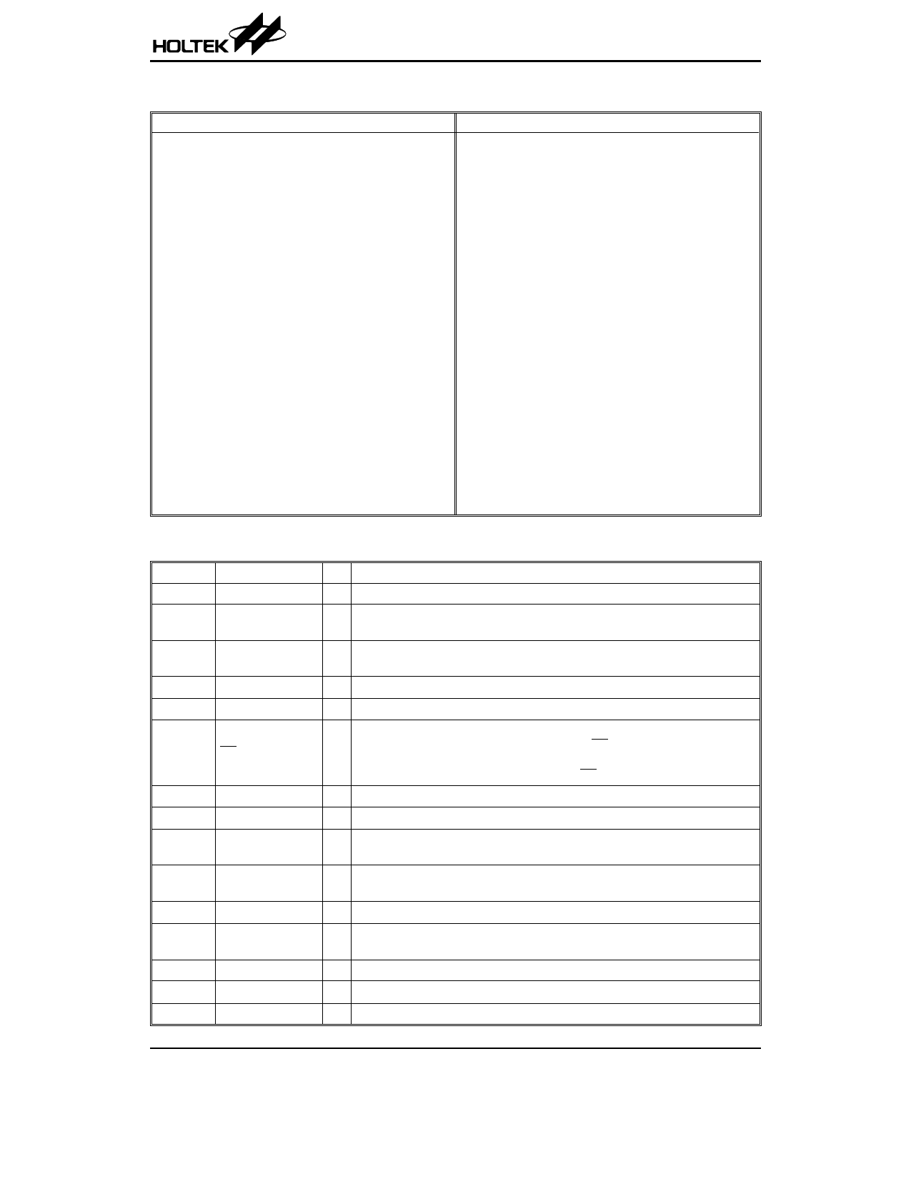
Pad Coordinates
Pad No.
1
2
3
4
5
6
7
8
9
10
11
12
13
14
15
16
17
18
19
20
21
22
23
24
25
26
X
-1110.000
-1110.000
-1110.000
-1110.000
-1110.000
-1165.900
-1110.000
-1110.000
-1110.000
-1110.000
-1110.000
-1110.000
-1110.000
-897.200
-782.500
-674.500
-566.500
-458.500
-350.500
-242.500
-134.500
-26.500
81.500
189.500
297.500
405.500
Y
555.300
450.300
345.300
240.300
135.300
9.800
-125.500
-230.500
-335.500
-440.500
-545.500
-650.500
-755.500
-560.300
-560.300
-560.300
-560.300
-560.300
-560.300
-560.300
-560.300
-560.300
-560.300
-560.300
-560.300
-560.300
Pad No.
27
28
29
30
31
32
33
34
35
36
37
38
39
40
41
42
43
44
45
46
47
48
49
50
51
X
977.250
977.250
977.250
977.250
977.250
977.250
977.250
977.250
977.250
977.250
977.250
977.250
977.250
977.250
405.500
297.500
189.500
81.500
-34.700
-173.950
-285.150
-390.150
-501.350
-606.350
-765.200
Unit: mm
Y
-720.000
-612.000
-504.000
-396.000
-288.000
-180.000
-55.150
49.850
173.350
281.350
389.350
497.350
605.350
713.350
545.400
545.400
545.400
545.400
545.400
684.850
684.850
684.850
684.850
684.850
726.350
Pin Description
Pin No.
Pin Name
I/O
Description
1~4
SW1~SW4
I 4-bit general purpose input port
5
DO
O
Output serial data at the falling edge of the shift clock, starting from low order
bit. This is an NMOS open-drain output pin.
6
DI
I
Input serial data at the rising edge of the shift clock, starting from the low order
bit.
7
NC
¾ No connection
8
CLK
I Reads serial data at the rising edge, and outputs data at the falling edge.
9
CS
Initializes serial interface at the rising or falling edge of the HT16511. Then it
I
waits to receive a command. Data input after CS has fallen is processed as a
command. While command data is processed, current processing is stopped,
and the serial interface is initialized. While CS is high, CLK is ignored.
10~13 K0~K3
I Keying data input to these pins is latched at the end of the display cycle.
14, 33, 45 VDD
¾ Posistive power supply
15~26
S1/K1~S12/K12
O
Segment or key source output pins (dual function). This is PMOS open-drain
and pull-low resistor output.
27~32,
35~36
S13/G16~S20/G9
O
Segment or Grid driver output pins. These pins are selectable for segment or
grid driving. This is PMOS open-drain and pull-low resistor output.
34
VEE
¾ VFD power supply
37~44 G8~G1
O
Grid driver output pins (Grid only). This is PMOS open-drain and pull-low re-
sistor output.
46~50 LED4~LED0
O LED driver output ports. This is a CMOS output pin.
51
VSS
¾ Negative power supply, ground
52
OSC
I Connected to an external resistor or an RC oscillator circuit.
Rev. 1.10
3
September 18, 2003
Share Link: 