HT16566 Ver la hoja de datos (PDF) - Holtek Semiconductor
Número de pieza
componentes Descripción
Fabricante
HT16566 Datasheet PDF : 8 Pages
| |||
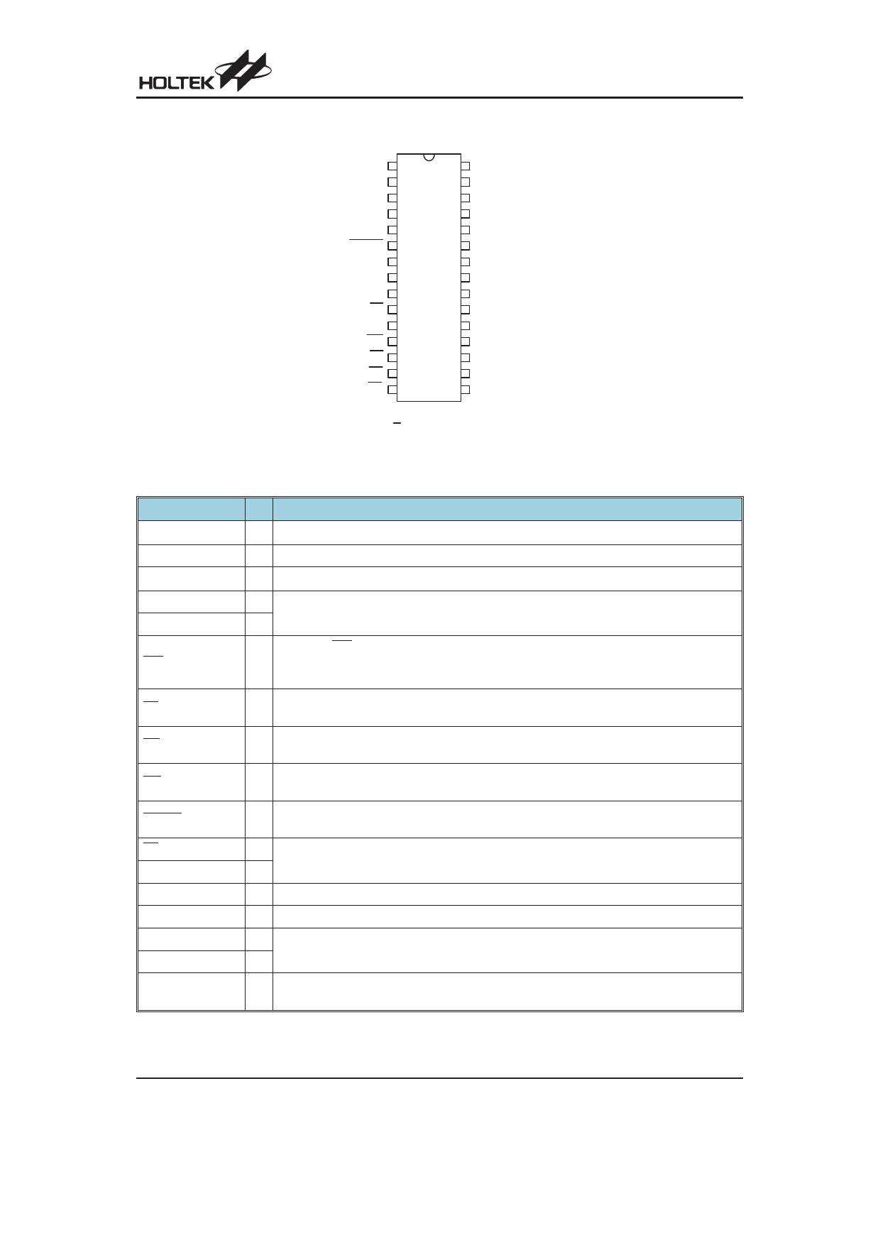
Pin Assignment
GR2
VCC
VDD
64H z
TEST
B LA N K
D IM 1
D IM 2
XT
XT
VSS
A /C
ZA
HS
MS
1
30
2
29
3
28
4
27
5
26
6
25
7
24
8
23
9
22
10
21
11
20
12
19
13
18
14
17
15
16
H T16566
3 0 S S O P -A
GR1
2a,2d,4a
2b,4b
2 f, 4 c
2 c , c o l*
2 c , c o l'*
2e,4e
2g,4g,4d
1d,3d
1e,3e
1c,3c
1g,3g
1 f, 3 f
1 b ,3 b
1a,3a
Note: ²*² col indicates a blink colon and col¢ indicates a continuous light colon.
Pin Description
Pin Name
VCC
VDD
VSS
DIM1
DIM2
A/C
ZA
HS
MS
BLANK
XT
XT
TEST
64Hz
GR1
GR2
1a,3a ~
2b,4b,4c
I/O
Description
¾ High voltage power supply pin.
O Built-in regulator voltage output pin for the device internal circuits.
¾ Ground pin.
I Illumination level control pins.
I Internally connected to pull-down resistors.
When the A/C pin is low, the internal circuits are reset.
I The reset pulse width should be more than 2ms.
Internally connected to a pull-high resistor.
I
Zero Adjustment pin.
Internally connected to a pull-high resistor.
I
Hour Adjustment pin.
Internally connected to a pull-high resistor.
I
Minute Adjustment pin.
Internally connected to a pull-high resistor.
I
When low the Blank input pin will extinguish the display.
Internally connected to a pull-down resistor.
O
Crystal oscillator pin
I
I IC test pin - should be left open or kept at a low level
O 64Hz signal output pin for oscillation frequency adjustment
O
Grid output pins for 1/2 duty VFD
O
O Segment output pins for 1/2 duty VFD
HT16566
Rev. 1.10
2
December 17, 2010
Share Link: 