HV76 Ver la hoja de datos (PDF) - Supertex Inc
Número de pieza
componentes Descripción
Fabricante
HV76 Datasheet PDF : 5 Pages
| |||
HV7620
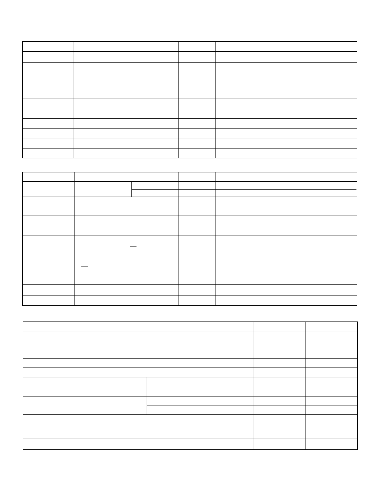
Electrical Characteristics (over recommended operating conditions unless noted)
DC Characteristics (VDD1 = 5V, VDD2 = 12V, VPP = 200V and TA = 25°C)
Symbol
Parameters
Min
Max
Units
Condition
IDD1
VDD1 supply current
5
mA
fCLK =10MHz
I
V supply current
DD2
DD2
20
mA
V = V max
DD2
DD2
fCLK = 10 MHz
I
High voltage supply current
PP
2
mA
All output high or low
IDD1Q
Quiescent VDD1 supply current
100
µA
All input = VDD1
IDD2Q
Quiescent VDD2 supply current
100
µA
All input = VDD1
VOH
High-level output
185
V
IO = -50mA
VOL
Low-level output
20
V
IO = 50mA
IIH
High-level logic input current
1.0
µA
VIN = VDD1
IIL
Low-level logic input current
-10
µA
VIN = 0V
VGG
HVGND to LVGND voltage difference
-1.0
1.0
V
AC Characteristics (Logic signal inputs and data inputs have tr, tf ≤ 5ns. VDD1 = 5V or 12V, VDD2 = 12V, VPP = 200V)
Symbol
fCLK
tWL, tWH
tSU
tH
tON, tOFF
tWLE
tDLE
tSLE
tDLF, tDLN
tCOF, tCON
tDLH
t
DHL
Parameters
Min
Clock frequency
VDD1 = 5V
VDD1 = 12V
Clock width high or low
40
Data set-up time
20
Data hold time
20
Time from LE to HVOUT
Width of LE pulse
25
Delay time clock to LE low to high
50
LE setup time before clock rises
20
BL or CS low to high to HVOUT
Clock to HVOUT
Delay time clock to data low to high
Delay time clock to data high to low
Max
10
5
275
250
275
100
100
Units
MHz
MHz
ns
ns
ns
ns
ns
ns
ns
ns
ns
ns
ns
Condition
Per register CL = 15pF
Per register CL = 15pF
CL = 15pF
CL = 15pF
C = 15pF
L
Recommended Operating Conditions
Symbol
VDD1
VDD2
VPP
VIH
VIL
fCLK
TA
I
OD
IGND(Vpp)
V
2
PP(SLEW)
Parameters
Logic supply voltage
12V supply voltage
High voltage supply voltage
High-level input voltage
Low-level input voltage
Clock frequency
VDD1 = 5V
Operating free-air temperature
VDD1 = 12V
Plastic
Ceramic
Allowable pulsed current through
ouptut diodes1
Allowable pulsed VPP or HVGND current1
Slew rate of V
PP
Min
4.5
10.8
50
VDD1-0.5V
0
-40
-55
Max
VDD2
13.2
200
VDD1
0.5
10
5
+85
+125
500
16
340
Unit
V
V
V
V
V
MHz
MHz
°C
°C
mA
A
V/µs
Notes:
1.The current pulse width = 500ns, duty cycle = 5%.
2.This device cannot be hot-switched for output frequency greater than 500Hz. For output frequency greater than 500Hz, VPP must be ramped.
2
Share Link: 